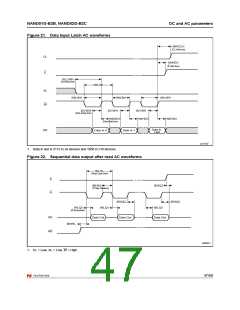
NAND01G-B2B, NAND02G-B2C
DC and AC parameters
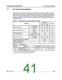
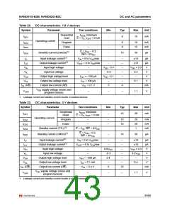
Table 22. DC characteristics, 1.8 V devices
Symbol
Parameter
Test conditions
Min
Typ
Max
Unit
Sequential
read
tRLRL minimum
IDD1
-
8
15
mA
E = VIL, OUT = 0 mA
I
Operating current
IDD2
IDD3
Program
Erase
–
–
-
-
8
8
15
15
mA
mA
E = VDD – 0.2,
WP = 0/VDD
IDD5
Standby current (CMOS)(1)
-
10
50
µA
ILI
ILO
Input leakage current(1)
Output leakage current(1)
Input high voltage
VIN = 0 to VDDmax
VOUT = 0 to VDDmax
–
-
–
–
–
–
–
–
4
±10
±10
µA
µA
V
-
VIH
VDD - 0.4
VDD + 0.3
0.4
VIL
Input low voltage
–
-0.3
V
VOH
VOL
Output high voltage level
Output low voltage level
Output low current (RB)
IOH = –100 µA
IOL = 100 µA
VOL = 0.1 V
VDD - 0.1
–
V
–
3
0.1
V
IOL (RB)
mA
VDD supply voltage (erase and
program lockout)
VLKO
–
–
–
1.1
V
1. Leakage current and standby current double in stacked devices.
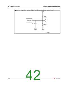
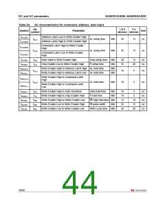
Table 23. DC characteristics, 3 V devices
Symbol
Parameter
Test conditions
Min
Typ
Max
Unit
Sequential
Read
tRLRL minimum
IDD1
–
10
20
mA
E = VIL, OUT = 0 mA
I
Operating current
IDD2
IDD3
Program
Erase
–
–
–
–
10
10
20
20
1
mA
mA
mA
I
Standby current (TTL)(1)
E = VIH, WP = 0/VDD
DD4
E = VDD – 0.2,
WP = 0/VDD
IDD5
Standby current (CMOS)(1)
–
10
50
µA
ILI
ILO
Input leakage current(1)
Output leakage current(1)
Input high voltage
VIN = 0 to VDDmax
VOUT = 0 to VDDmax
–
–
–
–
–
±10
±10
µA
µA
V
VIH
0.8VDD
-0.3
2.4
–
–
VDD + 0.3
0.2VDD
–
VIL
Input low voltage
–
–
V
VOH
VOL
Output high voltage level
Output low voltage level
Output low current (RB)
IOH = –400 µA
IOL = 2.1 mA
VOL = 0.4 V
–
V
–
0.4
V
IOL (RB)
8
10
mA
VDD supply voltage (erase and
program lockout)
VLKO
–
–
–
1.7
V
1. Leakage current and standby current double in stacked devices.
43/60

 NUMONYX [ NUMONYX B.V ]