Device operations
NAND01G-B2B, NAND02G-B2C
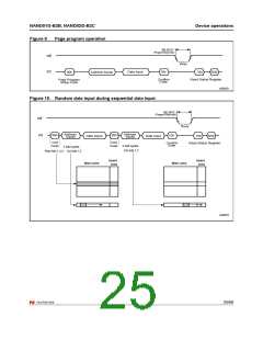
6.5
Cache program
The cache program operation is used to improve the programming throughput by
programming data using the cache register. The cache program operation can only be used
within one block. The cache register allows new data to be input while the previous data that
was transferred to the page buffer is programmed into the memory array.
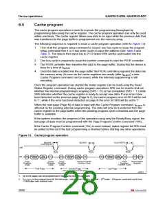
The following sequence is required to issue a cache program operation (refer to Figure 13):
1. First of all the program setup command is issued: one bus cycle to issue the program
setup command then 4 or 5 bus write cycles to input the address (see Table 6 and
Table 7). The data is then input (up to 2112 bytes/1056 words) and loaded into the
cache register
2. One bus cycle is required to issue the confirm command to start the P/E/R controller
3. The P/E/R controller then transfers the data to the page buffer. During this the device is
busy for a time of t
BLBH5
4. Once the data is loaded into the page buffer the P/E/R controller programs the data into
the memory array. As soon as the cache registers are empty (after t ) a new
BLBH5
Cache Program command can be issued, while the internal programming is still
executing.
Once the program operation has started the status register can be read using the Read
Status Register command. During cache program operations SR5 can be read to find out
whether the internal programming is ongoing (SR5 = ‘0’) or has completed (SR5 = ‘1’) while
SR6 indicates whether the cache register is ready to accept new data. If any errors have
been detected on the previous page (Page N-1), the cache program error bit SR1 will be set
to ‘1', while if the error has been detected on page N the error bit SR0 will be set to '1’.
When the next page (Page N) of data is input with the Cache Program command, t
is
BLBH5
affected by the pending internal programming. The data will only be transferred from the
cache register to the page buffer when the pending program cycle is finished and the page
buffer is available.
If the system monitors the progress of the operation using only the Ready/Busy signal, the
last page of data must be programmed with the Page Program Confirm command (10h).
If the Cache Program Confirm command (15h) is used instead, status register bit SR5 must
be polled to find out if the last programming is finished before starting any other operations.
Figure 13. Cache program operation
tBLBH5
tBLBH5
tCACHEPG
(Cache Busy time)
RB
Busy
Busy
10h
Busy
Address Data
Inputs Inputs
Address Data
Inputs Inputs
Address Data
I/O
80h
15h
80h
15h
80h
70h SR0
Inputs
Inputs
Cache Program
Confirm Code
Page
Program
Confirm Code
Read Status
Register
Page
Program
Code
Cache
Page
Program Program
Code
Code
First Page
Second Page
Last Page
(can be repeated up to 63 times)
ai08672
1. Up to 64 pages can be programmed in one cache program operation.
2. tCACHEPG is the program time for the last page + the program time for the (last − 1)th page − (Program command cycle time
+ Last page data loading time).
28/60

 NUMONYX [ NUMONYX B.V ]