NAND01G-B2B, NAND02G-B2C
Command set
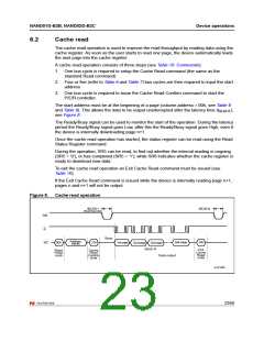
5
Command set
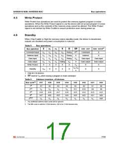
All bus write operations to the device are interpreted by the command interface. The
commands are input on I/O0-I/O7 and are latched on the rising edge of Write Enable when
the Command Latch Enable signal is High. Device operations are selected by writing
specific commands to the command register. The two-step command sequences for
program and erase operations are imposed to maximize data security.
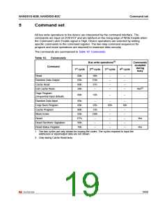
The commands are summarized in Table 10: Commands.
Table 10. Commands
Bus write operations(1)
Commands
accepted
during
Command
1st cycle
2nd cycle
3rd cycle
4th cycle
busy
Read
00h
05h
00h
34h
30h
E0h
31h
–
–
–
–
–
–
–
–
–
Random Data Output
Cache Read
Exit Cache Read
Yes(2)
Page Program
80h
10h
–
–
(Sequential Input default)
Random Data Input
Copy Back Program
Cache Program
Block Erase
85h
00h
80h
60h
FFh
90h
70h
–
35h
15h
D0h
–
–
85h
–
–
10h
–
–
–
Reset
–
–
Yes
Yes
Read Electronic Signature
Read Status Register
–
–
–
–
–
–
1. The bus cycles are only shown for issuing the codes. The cycles required to input the
addresses or input/output data are not shown.
2. Only during Cache Read busy.
19/60

 NUMONYX [ NUMONYX B.V ]