NAND01G-B2B, NAND02G-B2C
Bus operations
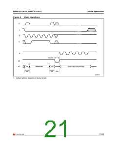
4.5
Write Protect
Write Protect bus operations are used to protect the memory against program or erase
operations. When the Write Protect signal is Low the device will not accept program or erase
operations and so the contents of the memory array cannot be altered. The Write Protect
signal is not latched by Write Enable to ensure protection even during power-up.
4.6
Standby
When Chip Enable is High the memory enters standby mode, the device is deselected,
outputs are disabled and power consumption is reduced.
Table 5.
Bus operations
Bus operation
E
AL
CL
R
W
WP
I/O0 - I/O7
I/O8 - I/O15(1)
Command input
Address input
Data input
VIL
VIL
VIL
VIL
X
VIL
VIH
VIL
VIL
X
VIH
VIL
VIL
VIH
VIH
VIH
Rising
Rising
Rising
VIH
X(2)
X
Command
Address
Data input
Data output
X
X
X
VIH
X
Data input
Data output
X
Data output
VIL Falling
Write Protect
X
X
X
X
X
VIL
VIL/VD
Standby
VIH
X
X
X
X
D
1. Only for x16 devices.
2. WP must be VIH when issuing a program or erase command.
Table 6.
Address insertion, x8 devices
Bus cycle(1)
I/O7
I/O6
I/O5
I/O4
I/O3
I/O2
I/O1
I/O0
1st
2nd
3rd
A7
VIL
A6
VIL
A5
VIL
A4
VIL
A3
A11
A15
A23
VIL
A2
A10
A14
A22
VIL
A1
A9
A0
A8
A19
A27
VIL
A18
A26
VIL
A17
A25
VIL
A16
A24
VIL
A13
A21
VIL
A12
A20
A28
4th
5th(2)
1. Any additional address input cycles will be ignored.
2. The fifth cycle is valid for 2-Gbit devices. A28 is for 2-Gbit devices only.
17/60

 NUMONYX [ NUMONYX B.V ]