Bus operations
NAND01G-B2B, NAND02G-B2C
4
Bus operations
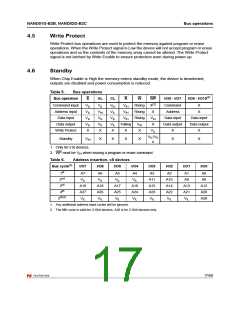
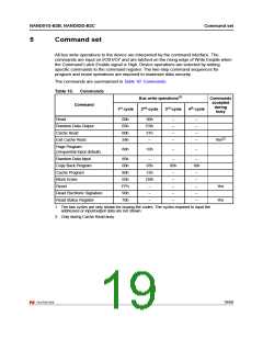
There are six standard bus operations that control the memory. Each of these is described
in this section, see Table 5: Bus operations, for a summary.
Typically, glitches of less than 5 ns on Chip Enable, Write Enable and Read Enable are
ignored by the memory and do not affect bus operations.
4.1
Command input
Command input bus operations are used to give commands to the memory. Commands are
accepted when Chip Enable is Low, Command Latch Enable is High, Address Latch Enable
is Low and Read Enable is High. They are latched on the rising edge of the Write Enable
signal.
Only I/O0 to I/O7 are used to input commands.
See Figure 19 and Table 24 for details of the timings requirements.
4.2
Address input
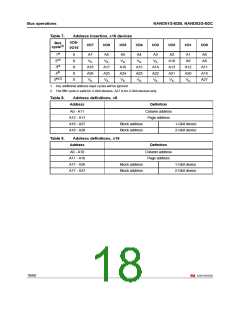
Address input bus operations are used to input the memory addresses. Four bus cycles are
required to input the addresses for 1-Gbit devices whereas five bus cycles are required for
the 2-Gbit device (refer to Table 6 and Table 7, Address insertion).
The addresses are accepted when Chip Enable is Low, Address Latch Enable is High,
Command Latch Enable is Low and Read Enable is High. They are latched on the rising
edge of the Write Enable signal. Only I/O0 to I/O7 are used to input addresses.
See Figure 20 and Table 24 for details of the timings requirements.
4.3
4.4
Data input
Data input bus operations are used to input the data to be programmed.
Data is accepted only when Chip Enable is Low, Address Latch Enable is Low, Command
Latch Enable is Low and Read Enable is High. The data is latched on the rising edge of the
Write Enable signal. The data is input sequentially using the Write Enable signal.
See Figure 21 and Table 24 and Table 25 for details of the timings requirements.
Data output
Data output bus operations are used to read: the data in the memory array, the status
register, the lock status, the electronic signature and the unique identifier.
Data is output when Chip Enable is Low, Write Enable is High, Address Latch Enable is Low,
and Command Latch Enable is Low. The data is output sequentially using the Read Enable
signal.
See Figure 22 and Table 25 for details of the timings requirements.
16/60

 NUMONYX [ NUMONYX B.V ]