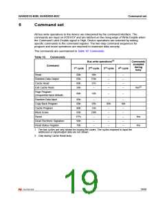
NAND01G-B2B, NAND02G-B2C
Signals description
3.7
Write Enable (W)
The Write Enable input, W, controls writing to the command interface, input address and
data latches. Both addresses and data are latched on the rising edge of Write Enable.
During power-up and power-down a recovery time of 10 µs (min) is required before the
command interface is ready to accept a command. It is recommended to keep Write Enable
High during the recovery time.
3.8
3.9
Write Protect (WP)
The Write Protect pin is an input that gives a hardware protection against unwanted program
or erase operations. When Write Protect is Low, V , the device does not accept any
program or erase operations.
IL
It is recommended to keep the Write Protect pin Low, V , during power-up and power-down.
IL
Ready/Busy (RB)
The Ready/Busy output, RB, is an open-drain output that can be used to identify if the P/E/R
controller is currently active. When Ready/Busy is Low, V , a read, program or erase
OL
operation is in progress. When the operation completes Ready/Busy goes High, V
.
OH
The use of an open-drain output allows the Ready/Busy pins from several memories to be
connected to a single pull-up resistor. A Low will then indicate that one, or more, of the
memories is busy.
Refer to the Section 11.1: Ready/Busy signal electrical characteristics for details on how to
calculate the value of the pull-up resistor.
During power-up and power-down a minimum recovery time of 10 µs is required before the
command interface is ready to accept a command. During this period the RB signal is Low,
V
.
OL
3.10
VDD supply voltage
V
provides the power supply to the internal core of the memory device. It is the main
DD
power supply for all operations (read, program and erase).
An internal voltage detector disables all functions whenever V is below V
(see
LKO
DD
Table 22 and Table 23) to protect the device from any involuntary program/erase during
power-transitions.
Each device in a system should have V decoupled with a 0.1 µF capacitor. The PCB track
DD
widths should be sufficient to carry the required program and erase currents.
3.11
VSS ground
Ground, V
ground.
is the reference for the power supply. It must be connected to the system
SS,
15/60

 NUMONYX [ NUMONYX B.V ]