®
Numonyx™ StrataFlash Embedded Memory (J3-65nm)
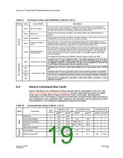
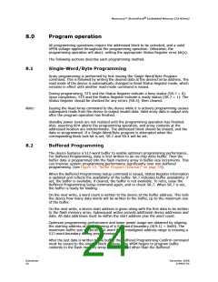
Table 8:
Command Bus Cycles (Sheet 2 of 2)
First Bus Cycle
Second Bus Cycle
Last Bus Cycle
Bus
Mode
Command
Cycles
(1)
(2)
(1)
(2)
(1)
(2)
Addr
Data
Addr
Data
Addr
Data
Block Erase
2
1
1
BA
0x20
BA
---
---
0xD0
---
---
---
---
---
---
Program/Erase Suspend
Program/Erase Resume
DnA
DnA
0xB0
0xD0
---
---
Lock Block
2
2
BA
BA
0x60
0x60
0xC0
0xC0
0xB8
0xEB
BA
BA
0x01
0xD0
---
---
---
---
---
---
---
Unlock Block
Program OTP register
Program Lock Register
STS Configuration
Extended Flash Interface
2
OTP-RA
LRA
BA
OTP-RA
LRA
OTP-D
---
2
LRD
---
2
BA
Register Data
Sub-Op code
---
(4)
> 2
WA
WA
WA
0xD0
Notes:
1.
First command cycle address should be the same as the operation’s target address.
DBA = Device Base Address
DnA = Address within the device.
IA = Identification code address offset.
CFI-A = Read CFI address offset.
WA = Word address of memory location to be written.
BA = Address within the block.
OTP-RA = OTP register address.
LRA = Lock Register address.
RCD = Read Configuration Register data on A[15:0].
ID = Identifier data.
2.
CFI-D = CFI data on DQ[15:0].
SRD = Status Register data.
WD = Word data.
N = Word count of data to be loaded into the write buffer.
OTP-D = OTP register data.
LRD = Lock Register data.
3.
4.
The second cycle of the Buffered Program Command is the word count of the data to be loaded into
the write buffer. This is followed by up to 512 words of data.Then the confirm command (0xD0) is
issued, triggering the array programming operation.
The second cycle is a Sub-Op-Code, the data written on third cycle is N-1; 1=<N<=512. The
subsequent cycles load data words into the program buffer at a specified address until word count is
achieved, after the data words are loaded, the final cycle is the confirm cycle 0xD0)
Datasheet
20
December 2008
319942-02

 NUMONYX [ NUMONYX B.V ]