AC Electrical Characteristics (Continued)
DS009219-9
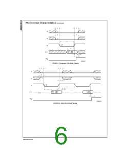
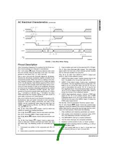
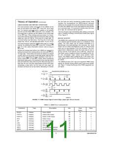
FIGURE 7. Data Word Write Timing
Pinout Description
(See Connection Diagrams) Pin numbers for the 24-pin sur-
3. Data is written and read via the data port (Pin 16 high).
face mount package are indicated in parentheses.
Pin 17 (10), Host Interrupt (HI) Output: This active-high
signal alerts the host (via a host interrupt service routine)
that an interrupt condition has occurred.
Pin 1 (17), Index (IN) Input: Receives optional index pulse
from the encoder. Must be tied high if not used. The index
position is read when Pins 1, 2, and 3 are low.
Pins 18 to 25, DAC Port (DAC0 to DAC7): Output port
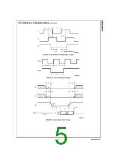
Pins 2 and 3 (18 and 19), Encoder Signal (A, B) Inputs:
Receive the two-phase quadrature signals provided by the
incremental encoder. When the motor is rotating in the posi-
tive (“forward”) direction, the signal at Pin 2 leads the signal
at Pin 3 by 90 degrees. Note that the signals at Pins 2 and 3
must remain at each encoder state (See Figure 9) for a mini-
mum of 8 clock periods in order to be recognized. Because
of a four-to-one resolution advantage gained by the method
of decoding the quadrature encoder signals, this corre-
sponds to a maximum encoder-state capture rate of 1.0 MHz
which is used in three different modes:
1. LM628 (8-bit output mode): Outputs latched data to the
DAC. The MSB is Pin 18 and the LSB is Pin 25.
2. LM628 (12-bit output mode): Outputs two, multiplexed
6-bit words. The less-significant word is output first. The
MSB is on Pin 18 and the LSB is on Pin 23. Pin 24 is
used to demultiplex the words; Pin 24 is low for the
less-significant word. The positive-going edge of the sig-
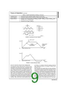
nal on Pin 25 is used to strobe the output data. Figure 8
shows the timing of the multiplexed signals.
=
=
(fCLK
8.0 MHz) or 750 kHz (fCLK
6.0 MHz). For other
3. LM629 (sign/magnitude outputs): Outputs a PWM sign
signal on Pin 18 (11 for surface mount), and a PWM
magnitude signal on Pin 19 (13 for surface mount). Pins
20 to 25 are not used in the LM629. Figure 11 shows the
PWM output signal format.
clock frequencies the encoder signals must also remain at
each state a minimum of 8 clock periods.
Pins 4 to 11 (20 to 24 and 2 to 4), Host I/O Port (D0 to D7):
Bi-directional data port which connects to host computer/
processor. Used for writing commands and data to the
LM628, and for reading the status byte and data from the
LM628, as controlled by CS (Pin 12), PS (Pin 16), RD (Pin
13), and WR (Pin 15).
Pin 26 (14), Clock (CLK) Input: Receives system clock.
Pin 27 (15), Reset (RST) Input: Active-low, positive-edge
triggered, resets the LM628 to the internal conditions shown
below. Note that the reset pulse must be logic low for a mini-
mum of 8 clock periods. Reset does the following:
Pin 12 (5), Chip Select (CS ) Input: Used to select the
LM628 for writing and reading operations.
1. Filter coefficient and trajectory parameters are zeroed.
Pin 13 (6), Read (RD ) Input: Used to read status and data.
Pin 14 (7), Ground (GND): Power-supply return pin.
2. Sets position error threshold to maximum value (7FFF
hex), and effectively executes command LPEI.
Pin 15 (8), Write (WR ) Input: Used to write commands and
data.
3. The SBPA/SBPR interrupt is masked (disabled).
4. The five other interrupts are unmasked (enabled).
5. Initializes current position to zero, or “home” position.
Pin 16 (9), Port Select (PS ) Input: Used to select com-
mand or data port. Selects command port when low, data
port when high. The following modes are controlled by Pin
16:
6. Sets derivative sampling interval to 2048/fCLK or 256 µs
for an 8.0 MHz clock.
1. Commands are written to the command port (Pin 16
low),
7. DAC port outputs 800 hex to “zero” a 12-bit DAC and
then reverts to 80 hex to “zero” an 8-bit DAC.
2. Status byte is read from command port (Pin 16 low), and
7
www.national.com

 NSC [ National Semiconductor ]