AC Electrical Characteristics (Continued)
=
=
=
=
(VDD and TA per Operating Ratings; fCLK 6 MHz; CLOAD 50 pF; Input Test Signal tr tf 10 ns)
Timing Interval
T#
Tested Limits
Units
Min
Max
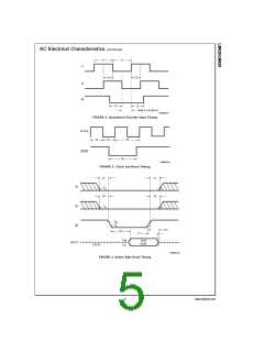
STATUS BYTE READ TIMING (See Figure 4)
Chip-Select Setup/Hold Time
Port-Select Setup Time
Port-Select Hold Time
T7
T8
0
ns
ns
ns
ns
ns
ns
30
30
T9
Read Data Access Time
Read Data Hold Time
T10
T11
T12
180
180
0
RD High to Hi-Z Time
COMMAND BYTE WRITE TIMING (See Figure 5)
Chip-Select Setup/Hold Time
Port-Select Setup Time
Port-Select Hold Time
T7
T8
0
ns
ns
ns
ns
ns
ns
ns
30
30
T9
Busy Bit Delay
T13
T14
T15
T16
(Note 3)
WR Pulse Width
100
50
Write Data Setup Time
Write Data Hold Time
120
DATA WORD READ TIMING (See Figure 6)
Chip-Select Setup/Hold Time
Port-Select Setup Time
Port-Select Hold Time
T7
T8
0
ns
ns
ns
ns
ns
ns
ns
ns
30
30
T9
Read Data Access Time
Read Data Hold Time
T10
T11
T12
T13
T17
180
0
RD High to Hi-Z Time
180
Busy Bit Delay
(Note 3)
Read Recovery Time
120
DATA WORD WRITE TIMING (See Figure 7)
Chip-Select Setup/Hold Time
Port-Select Setup Time
Port-Select Hold Time
T7
T8
0
ns
ns
ns
ns
ns
ns
ns
ns
30
30
T9
Busy Bit Delay
T13
T14
T15
T16
T18
(Note 3)
WR Pulse Width
100
50
Write Data Setup Time
Write Data Hold Time
120
120
Write Recovery Time
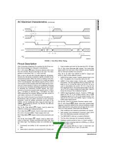
Note 1: Absolute Maximum Ratings indicate limits beyond which damage to the device may occur. DC and AC electrical specifications do not apply when operating
the device beyond the above Operating Ratings.
Note 2: When operating at ambient temperatures above 70˚C, the device must be protected against excessive junction temperatures. Mounting the package on a
printed circuit board having an area greater than three square inches and surrounding the leads and body with wide copper traces and large, uninterrupted areas of
copper, such as a ground plane, suffices. The 28-pin DIP (N) and the 24-pin surface mount package (M) are molded plastic packages with solid copper lead frames.
Most of the heat generated at the die flows from the die, through the copper lead frame, and into copper traces on the printed circuit board. The copper traces act
as a heat sink. Double-sided or multi-layer boards provide heat transfer characteristics superior to those of single-sided boards.
Note 3: In order to read the busy bit, the status byte must first be read. The time required to read the busy bit far exceeds the time the chip requires to set the busy
bit. It is, therefore, impossible to test actual busy bit delay. The busy bit is guaranteed to be valid as soon as the user is able to read it.
www.national.com
4

 NSC [ National Semiconductor ]