Absolute Maximum Ratings (Note 1)
If Military/Aerospace specified devices are required,
please contact the National Semiconductor Sales Office/
Distributors for availability and specifications.
(TA ≤ 85˚C, (Note 2)
605 mW
2000V
ESD Tolerance
=
=
(CZAP 120 pF, RZAP 1.5k)
Operating Ratings
Voltage at Any Pin with
Respect to GND
−0.3V to +7.0V
< <
−40˚C TA +85˚C
Temperature Range
Clock Frequency:
LM628N-6, LM629N-6,
LM629M-6
Ambient Storage Temperature
Lead Temperature
−65˚C to +150˚C
28-pin Dual In-Line
<
<
1.0 MHz fCLK 6.0 MHz
Package (Soldering, 4 sec.)
24-pin Surface Mount
260˚C
300˚C
LM628N-8, LM629N-8,
LM629M-8
<
<
1.0 MHz fCLK 8.0 MHz
Package (Soldering, 10 sec.)
Maximum Power Dissipation
<
<
VDD Range
4.5V VDD 5.5V
DC Electrical Characteristics
=
(VDD and TA per Operating Ratings; fCLK 6 MHz)
Symbol Parameter
Conditions
Tested Limits
Units
Min
Max
IDD
Supply Current
Outputs Open
110
mA
INPUT VOLTAGES
VIH
VIL
IIN
Logic 1 Input Voltage
Logic 0 Input Voltage
Input Currents
2.0
−10
2.4
V
V
0.8
10
0 ≤ VIN ≤ VDD
µA
OUTPUT VOLTAGES
=
VOH
VOL
IOUT
Logic 1
IOH −1.6 mA
V
V
=
Logic 0
IOL 1.6 mA
0.4
10
TRI-STATE® Output Leakage Current
0 ≤ VOUT ≤ VDD
−10
µA
AC Electrical Characteristics
=
=
=
=
(VDD and TA per Operating Ratings; fCLK 6 MHz; CLOAD 50 pF; Input Test Signal tr tf 10 ns)
Timing Interval
T#
Tested Limits
Units
Min
Max
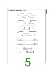
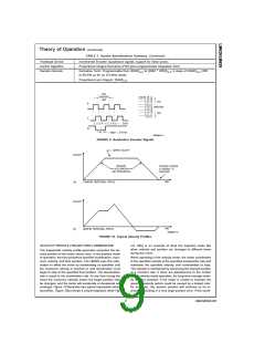
ENCODER AND INDEX TIMING (See Figure 2)
Motor-Phase Pulse Width
T1
µs
Dwell-Time per State
T2
T3
µs
µs
Index Pulse Setup and Hold
(Relative to A and B Low)
0
CLOCK AND RESET TIMING (See Figure 3)
Clock Pulse Width
LM628N-6, LM629N-6, LM629M-6
LM628N-8, LM629N-8, LM629M-8
Clock Period
T4
T4
78
57
ns
ns
LM628N-6, LM629N-6, LM629M-6
LM628N-8, LM629N-8, LM629M-8
Reset Pulse Width
T5
T5
T6
166
125
ns
ns
µs
3
www.national.com

 NSC [ National Semiconductor ]