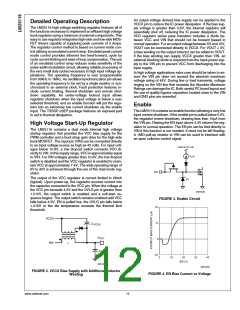
voltage momentarily dips out of regulation. When a fault is
detected (VCC under-voltage, UVLO pin < 1.215, or EN = 0V)
the soft-start capacitor is discharged. Once the fault condition
is no longer present, a new soft-start sequence begins.
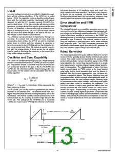
OUTPUT INDUCTOR
The inductor value is determined based on the operating fre-
quency, load current, ripple current and the input and output
voltages.
HO Ouput
The LM25116 contains a high current, high-side driver and
associated high voltage level shift. This gate driver circuit
works in conjunction with an external diode and bootstrap ca-
pacitor. A 1µF ceramic capacitor, connected with short traces
between the HB pin and SW pin, is recommended. During the
off-time of the high-side MOSFET, the SW pin voltage is ap-
proximately -0.5V and the bootstrap capacitor charges from
VCC through the external bootstrap diode. When operating
with a high PWM duty cycle, the buck switch will be forced off
each cycle for 450ns to ensure that the bootstrap capacitor is
recharged.
The LO and HO outputs are controlled with an adaptive dead-
time methodology which insures that both outputs are never
enabled at the same time. When the controller commands HO
to be enabled, the adaptive block first disables LO and waits
for the LO voltage to drop below approximately 25% of VCC.
HO is then enabled after a small delay. Similarly, LO is en-
abled once HO has discharged. This methodology insures
adequate dead-time for any size MOSFET.
30015645
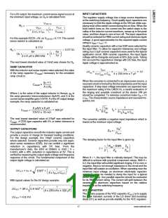
FIGURE 9. Inductor Current
Knowing the switching frequency (fSW), maximum ripple cur-
rent (IPP), maximum input voltage (VIN(MAX)) and the nominal
output voltage (VOUT), the inductor value can be calculated:
Thermal Protection
Internal thermal shutdown circuitry is provided to protect the
integrated circuit in the event the maximum junction temper-
ature is exceeded. When activated, typically at 170°C, the
controller is forced into a low power reset state, disabling the
output driver and the bias regulator. This is designed to pre-
vent catastrophic failures from accidental device overheating.
The maximum ripple current occurs at the maximum input
voltage. Typically, IPP is 20% to 40% of the full load current.
When running diode emulation mode, the maximum ripple
current should be less than twice the minimum load current.
For full synchronous operation, higher ripple current is ac-
ceptable. Higher ripple current allows for a smaller inductor
size, but places more of a burden on the output capacitor to
smooth the ripple current for low output ripple voltage. For this
example, 40% ripple current was chosen for a smaller sized
inductor.
Application Information
EXTERNAL COMPONENTS
The procedure for calculating the external components is il-
lustrated with the following design example. The Bill of Mate-
rials for this design is listed in Table 1. The circuit shown in
Figure 15 is configured for the following specifications:
•
•
•
•
Output voltage = 5V
Input voltage = 7V to 42V
Maximum load current = 7A
Switching frequency = 250kHz
The nearest standard value of 6µH will be used. The inductor
must be rated for the peak current to prevent saturation. Dur-
ing normal operation, the peak current occurs at maximum
load current plus maximum ripple. During overload conditions
with properly scaled component values, the peak current is
limited to VCS(TH) / RS (See next section). At the maximum
input voltage with a shorted output, the valley current must fall
below VCS(TH) / RS before the high-side MOSFET is allowed
to turn on. The peak current in steady state will increase to
VIN(MAX) x tON(min) / L above this level. The chosen inductor
must be evaluated for this condition, especially at elevated
temperature where the saturation current rating may drop sig-
nificantly.
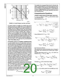
Simplified equations are used as a general guideline for the
design method. Comprehensive equations are provided at
the end of this section.
TIMING RESISTOR
RT sets the oscillator switching frequency. Generally, higher
frequency applications are smaller but have higher losses.
Operation at 250kHz was selected for this example as a rea-
sonable compromise for both small size and high efficiency.
The value of RT for 250kHz switching frequency can be cal-
culated as follows:
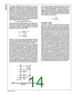
CURRENT SENSE RESISTOR
The current limit is set by the current sense resistor value
(RS).
The nearest standard value of 12.4kΩ was chosen for RT.
www.national.com
16

 NSC [ National Semiconductor ]