The regulator has an exposed thermal pad to aid power dis-
sipation. Selecting MOSFETs with exposed pads will aid the
power dissipation of these devices. The resulting power loss-
es are primarily in the switching MOSFETs. Careful attention
to RDS(ON) at high temperature should be observed. Also, at
250 kHz, a MOSFET with low gate capacitance will result in
lower switching losses.
Comprehensive Equations
CURRENT SENSE RESISTOR AND RAMP CAPACITOR
T = 1 / fSW, gm = 5µA/V, A = 10V/V. IOUT is the maximum output
current at current limit.
General Method for VOUT < 5V:
30015665
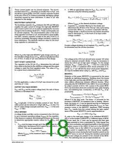
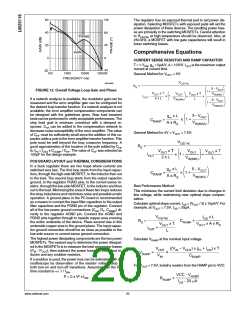
FIGURE 12. Overall Voltage Loop Gain and Phase
If a network analyzer is available, the modulator gain can be
measured and the error amplifier gain can be configured for
the desired loop transfer function. If a network analyzer is not
available, the error amplifier compensation components can
be designed with the guidelines given. Step load transient
tests can be performed to verify acceptable performance. The
step load goal is minimum overshoot with a damped re-
sponse. CHF can be added to the compensation network to
decrease noise susceptibility of the error amplifier. The value
of CHF must be sufficiently small since the addition of this ca-
pacitor adds a pole in the error amplifier transfer function. This
pole must be well beyond the loop crossover frequency. A
good approximation of the location of the pole added by CHF
is: fP2 = fZEA x CCOMP / CHF. The value of CHF was selected as
100pF for the design example.
General Method for 5V < VOUT < 7.5V:
PCB BOARD LAYOUT and THERMAL CONSIDERATIONS
In a buck regulator there are two loops where currents are
switched very fast. The first loop starts from the input capac-
itors, through the high-side MOSFET, to the inductor then out
to the load. The second loop starts from the output capacitor
ground, to the regulator PGND pins, to the current sense re-
sistor, through the low-side MOSFET, to the inductor and then
out to the load. Minimizing the area of these two loops reduces
the stray inductance and minimizes noise and possible erratic
operation. A ground plane in the PC board is recommended
as a means to connect the input filter capacitors to the output
filter capacitors and the PGND pin of the regulator. Connect
all of the low power ground connections (CSS, RT, CRAMP) di-
rectly to the regulator AGND pin. Connect the AGND and
PGND pins together through to topside copper area covering
the entire underside of the device. Place several vias in this
underside copper area to the ground plane. The input capac-
itor ground connection should be as close as possible to the
low-side source or current sense ground connection.
Best Performance Method:
This minimizes the current limit deviation due to changes in
line voltage, while maintaining near optimal slope compen-
sation.
Calculate optimal slope current, IOS = (VOUT / 3) x 10µA/V. For
example, at VOUT = 7.5V, IOS = 25µA.
The highest power dissipating components are the two power
MOSFETs. The easiest way to determine the power dissipat-
ed in the MOSFETs is to measure the total conversion losses
(PIN - POUT), then subtract the power losses in the output in-
ductor and any snubber resistors.
Calculate VRAMP at the nominal input voltage.
If a snubber is used, the power loss can be estimated with an
oscilloscope by observation of the resistor voltage drop at
both turn-on and turn-off transitions. Assuming that the RC
For VOUT > 7.5V, install a resistor from the RAMP pin to VCC.
time constant is << 1 / fSW
.
P = C x V2 x fSW
www.national.com
20

 NSC [ National Semiconductor ]