tion pulse detection. A 5V amplitude signal and 100pF cou-
pling capacitor are recommended. The free-running frequen-
cy should be set nominally 15% below the external clock.
Synchronizing above twice the free-running frequency may
result in abnormal behavior of the pulse width modulator.
UVLO
An under-voltage lockout pin is provided to disable the regu-
lator without entering shutdown. If the UVLO pin is pulled
below 1.215V, the regulator enters a standby mode of oper-
ation with the soft-start capacitor discharged and outputs
disabled, but with the VCC regulator running. If the UVLO in-
put is pulled above 1.215V, the controller will resume normal
operation. A voltage divider from input to ground can be used
to set a VIN threshold to disable the supply in brown-out con-
ditions or for low input faults. The UVLO pin has a 5µA internal
pull up current that allows this pin to left open if the input un-
der-voltage lockout function is not needed.
Error Amplifier and PWM
Comparator
The internal high-gain error amplifier generates an error sig-
nal proportional to the difference between the regulated out-
put voltage and an internal precision reference (1.215V). The
output of the error amplifier is connected to the COMP pin
allowing the user to provide loop compensation components,
generally a type II network. This network creates a pole at
very low frequency, a mid-band zero, and a noise reducing
high frequency pole. The PWM comparator compares the
emulated current sense signal from the RAMP generator to
the error amplifier output voltage at the COMP pin.
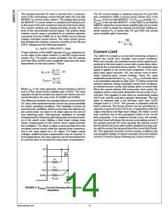
The UVLO pin can also be used to implement a “hiccup” cur-
rent limit. If a current limit fault exists for more than 256
consecutive clock cycles, the UVLO pin will be internally
pulled down to 200mV and then released. A capacitor to
ground connected to the UVLO pin will set the timing for hic-
cup mode current limit. When this feature is used in conjunc-
tion with the voltage divider, a diode across the top resistor
may be used to discharge the capacitor in the event of an
input under-voltage condition.
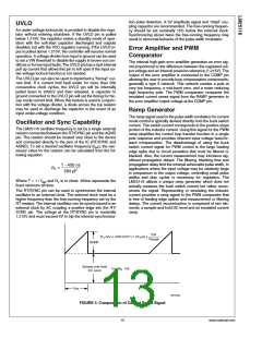
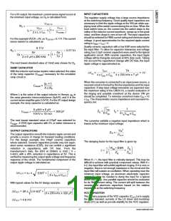
Ramp Generator
The ramp signal used in the pulse width modulator for current
mode control is typically derived directly from the buck switch
current. This switch current corresponds to the positive slope
portion of the inductor current. Using this signal for the PWM
ramp simplifies the control loop transfer function to a single
pole response and provides inherent input voltage feed-for-
ward compensation. The disadvantage of using the buck
switch current signal for PWM control is the large leading
edge spike due to circuit parasitics that must be filtered or
blanked. Also, the current measurement may introduce sig-
nificant propagation delays. The filtering, blanking time and
propagation delay limit the minimal achievable pulse width. In
applications where the input voltage may be relatively large
in comparison to the output voltage, controlling small pulse
widths and duty cycles is necessary for regulation. The
LM25116 utilizes a unique ramp generator which does not
actually measure the buck switch current but rather recon-
structs the signal. Representing or emulating the inductor
current provides a ramp signal to the PWM comparator that
is free of leading edge spikes and measurement or filtering
delays. The current reconstruction is comprised of two ele-
ments, a sample-and-hold DC level and an emulated current
ramp.
Oscillator and Sync Capability
The LM25116 oscillator frequency is set by a single external
resistor connected between the RT/SYNC pin and the AGND
pin. The resistor should be located very close to the device
and connected directly to the pins of the IC (RT/SYNC and
AGND). To set a desired oscillator frequency (fSW), the nec-
essary value for the resistor can be calculated from the fol-
lowing equation:
Where T = 1 / fSW and RT is in ohms. 450ns represents the
fixed minimum off time.
The RT/SYNC pin can be used to synchronize the internal
oscillator to an external clock. The external clock must be a
higher frequency than the free-running frequency set by the
RT resistor. The internal oscillator can be synchronized to an
external clock by AC coupling a positive edge into the RT/
SYNC pin. The voltage at the RT/SYNC pin is nominally
1.215V and must exceed 4V to trip the internal synchroniza-
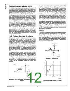
30015646
FIGURE 5. Composition of Current Sense Signal
13
www.national.com

 NSC [ National Semiconductor ]