PSW = 0.5 x VIN x IO x (tR + tF) x fSW
Where tR and tF are the rise and fall times of the MOSFET.
Switching loss is calculated for the high-side MOSFET only.
Switching loss in the low-side MOSFET is negligible because
the body diode of the low-side MOSFET turns on before the
MOSFET itself, minimizing the voltage from drain to source
before turn-on. For this example, the maximum drain-to-
source voltage applied to either MOSFET is 42V. VCC pro-
vides the drive voltage at the gate of the MOSFETs. The
selected MOSFETs must be able to withstand 42V plus any
ringing from drain to source, and be able to handle at least
VCC plus ringing from gate to source. A good choice of MOS-
FET for the 42V input design example is the Si7850DP. It has
an RDS(ON) of 20mΩ, total gate charge of 14nC, and rise and
fall times of 10ns and 12ns respectively. In applications where
a high step-down ratio is maintained for normal operation, ef-
ficiency may be optimized by choosing a high-side MOSFET
30015663
with lower Qg, and low-side MOSFET with lower RDS(ON)
.
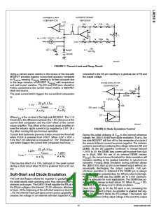
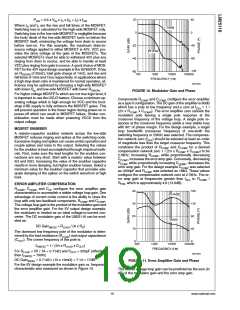
FIGURE 10. Modulator Gain and Phase
For higher voltage MOSFETs which are not true logic level, it
is important to use the UVLO feature. Choose a minimum op-
erating voltage which is high enough for VCC and the boot-
strap (HB) supply to fully enhance the MOSFET gates. This
will prevent operation in the linear region during power-on or
power-off which can result in MOSFET failure. Similar con-
sideration must be made when powering VCCX from the
output voltage.
Components RCOMP and CCOMP configure the error amplifier
as a type II configuration. The DC gain of the amplifier is 80dB
which has a pole at low frequency and a zero at fZEA = 1 /
(2π x RCOMP x CCOMP). The error amplifier zero cancels the
modulator pole leaving a single pole response at the
crossover frequency of the voltage loop. A single pole re-
sponse at the crossover frequency yields a very stable loop
with 90° of phase margin. For the design example, a target
loop bandwidth (crossover frequency) of one-tenth the
switching frequency or 25kHz was selected. The compensa-
tion network zero (fZEA) should be selected at least an order
of magnitude less than the target crossover frequency. This
constrains the product of RCOMP and CCOMP for a desired
compensation network zero 1 / (2π x RCOMP x CCOMP) to be
2.5kHz. Increasing RCOMP, while proportionally decreasing
CCOMP, increases the error amp gain. Conversely, decreasing
RCOMP while proportionally increasing CCOMP, decreases the
error amp gain. For the design example CCOMP was selected
as 3300pF and RCOMP was selected as 18kΩ. These values
configure the compensation network zero at 2.7kHz. The er-
MOSFET SNUBBER
A resistor-capacitor snubber network across the low-side
MOSFET reduces ringing and spikes at the switching node.
Excessive ringing and spikes can cause erratic operation and
couple spikes and noise to the output. Selecting the values
for the snubber is best accomplished through empirical meth-
ods. First, make sure the lead lengths for the snubber con-
nections are very short. Start with a resistor value between
5Ω and 50Ω. Increasing the value of the snubber capacitor
results in more damping, but higher snubber losses. Select a
minimum value for the snubber capacitor that provides ade-
quate damping of the spikes on the switch waveform at high
load.
ror amp gain at frequencies greater than fZEA is: RCOMP
RFB2, which is approximately 4.8 (13.6dB).
/
ERROR AMPLIFIER COMPENSATION
RCOMP, CCOMP and CHF configure the error amplifier gain
characteristics to accomplish a stable voltage loop gain. One
advantage of current mode control is the ability to close the
loop with only two feedback components, RCOMP and CCOMP
.
The voltage loop gain is the product of the modulator gain and
the error amplifier gain. For the 5V output design example,
the modulator is treated as an ideal voltage-to-current con-
verter. The DC modulator gain of the LM25116 can be mod-
eled as:
DC Gain(MOD) = RLOAD / (A x RS)
The dominant low frequency pole of the modulator is deter-
mined by the load resistance (RLOAD) and output capacitance
(COUT). The corner frequency of this pole is:
fP(MOD) = 1 / (2π x RLOAD x COUT
)
For RLOAD = 5V / 7A = 0.714Ω and COUT = 320µF (effective)
then fP(MOD) = 700Hz
30015664
DC Gain(MOD) = 0.714Ω / (10 x 10mΩ) = 7.14 = 17dB
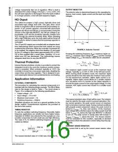
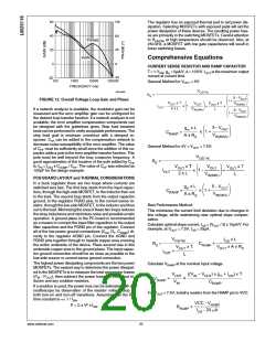
FIGURE 11. Error Amplifier Gain and Phase
For the 5V design example the modulator gain vs. frequency
characteristic was measured as shown in Figure 10.
The overall voltage loop gain can be predicted as the sum (in
dB) of the modulator gain and the error amp gain.
19
www.national.com

 NSC [ National Semiconductor ]