These current peaks can be several amperes. The recom-
mended value of CVCC should be no smaller than 0.47µF, and
should be a good quality, low ESR, ceramic capacitor located
at the pins of the IC to minimize potentially damaging voltage
transients caused by trace inductance. A value of 1µF was
selected for this design.
2. 2. With an appropriate value for RUV2, RUV1 can be
selected using the following equation:
BOOTSTRAP CAPACITOR
Where VIN(MIN) is the desired shutdown voltage.
The bootstrap capacitor (CHB) between the HB and SW pins
supplies the gate current to charge the high-side MOSFET
gate at each cycle’s turn-on as well as supplying the recovery
charge for the bootstrap diode (D1). These current peaks can
be several amperes. The recommended value of the boot-
strap capacitor is at least 0.1µF, and should be a good quality,
low ESR, ceramic capacitor located at the pins of the IC to
minimize potentially damaging voltage transients caused by
trace inductance. The absolute minimum value for the boot-
strap capacitor is calculated as:
3. Capacitor CFT provides filtering for the divider and
determines the off-time of the “hiccup” duty cycle during
current limit. When CFT is used in conjunction with the
voltage divider, a diode across the top resistor should be
used to discharge CFT in the event of an input under-
voltage condition.
If under-voltage shutdown is not required, RUV1 and RUV2 can
be eliminated and the off-time becomes:
Where Qg is the high-side MOSFET gate charge and ΔVHB is
the tolerable voltage droop on CHB, which is typically less than
5% of VCC. A value of 1µF was selected for this design.
The voltage at the UVLO pin should never exceed 16V when
using an external set-point divider. It may be necessary to
clamp the UVLO pin at high input voltages. For the design
example, RUV2 = 102kΩ and RUV1 = 21kΩ for a shut-down
voltage of 6.6V. If sustained short circuit protection is re-
quired, CFT ≥ 1µF will limit the short circuit power dissipation.
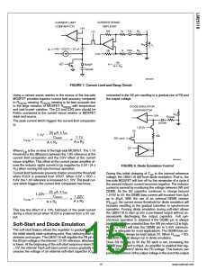
SOFT START CAPACITOR
The capacitor at the SS pin (CSS) determines the soft-start
time, which is the time for the reference voltage and the output
voltage to reach the final regulated value. The value of CSS
for a given time is determined from:
D2 may be installed when using CFT with RUV1 and RUV2
.
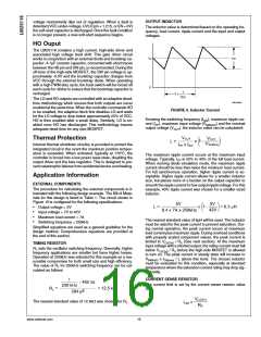
MOSFETs
Selection of the power MOSFETs is governed by the same
tradeoffs as switching frequency. Breaking down the losses
in the high-side and low-side MOSFETs is one way to deter-
mine relative efficiencies between different devices. When
using discrete SO-8 MOSFETs the LM25116 is most efficient
for output currents of 2A to 10A. Losses in the power MOS-
FETs can be broken down into conduction loss, gate charging
loss, and switching loss. Conduction, or I2R loss PDC, is ap-
proximately:
For this application, a value of 0.01µF was chosen for a soft-
start time of 1.2ms.
OUTPUT VOLTAGE DIVIDER
RFB1 and RFB2 set the output voltage level, the ratio of these
resistors is calculated from:
PDC(HO-MOSFET) = D x (IO2 x RDS(ON) x 1.3)
PDC(LO-MOSFET) = (1 - D) x (IO2 x RDS(ON) x 1.3)
Where D is the duty cycle. The factor 1.3 accounts for the
increase in MOSFET on-resistance due to heating. Alterna-
tively, the factor of 1.3 can be ignored and the on-resistance
of the MOSFET can be estimated using the RDS(ON) vs Tem-
perature curves in the MOSFET datasheet. Gate charging
loss, PGC, results from the current driving the gate capaci-
tance of the power MOSFETs and is approximated as:
RFB1 is typically 1.21kΩ for a divider current of 1mA. The di-
vider current can be reduced to 100µA with RFB1=12.1kΩ. For
the 5V output design example used here, RFB1 = 1.21kΩ and
RFB2 = 3.74kΩ.
UVLO DIVIDER
PGC = n x VCC x Qg x fSW
A voltage divider and filter can be connected to the UVLO pin
to set a minimum operating voltage VIN(MIN) for the regulator.
If this feature is required, the following procedure can be used
to determine appropriate resistor values for RUV2, RUV1 and
Qg refer to the total gate charge of an individual MOSFET,
and ‘n’ is the number of MOSFETs. If different types of MOS-
FETs are used, the ‘n’ term can be ignored and their gate
charges summed to form a cumulative Qg. Gate charge loss
differs from conduction and switching losses in that the actual
dissipation occurs in the LM25116 and not in the MOSFET
itself. Further loss in the LM25116 is incurred as the gate
driving current is supplied by the internal linear regulator.
Switching loss occurs during the brief transition period as the
MOSFET turns on and off. During the transition period both
current and voltage are present in the channel of the MOS-
FET. The switching loss can be approximated as:
CFT
.
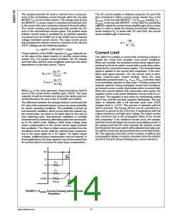
1. RUV2 must be large enough such that in the event of a
current limit, the internal UVLO switch can pull UVLO <
200mV. This can be guaranteed if:
RUV2 > 500 x VIN(MAX)
Where VIN(MAX) is the maximum input voltage and RUV2
is in ohms.
www.national.com
18

 NSC [ National Semiconductor ]