The sample-and-hold DC level is derived from a measure-
ment of the recirculating current through either the low-side
MOSFET or current sense resistor. The voltage level across
the MOSFET or sense resistor is sampled and held just prior
to the onset of the next conduction interval of the buck switch.
The current sensing and sample-and-hold provide the DC
level of the reconstructed current signal. The positive slope
inductor current ramp is emulated by an external capacitor
connected from the RAMP pin to the AGND and an internal
voltage controlled current source. The ramp current source
that emulates the inductor current is a function of the VIN and
VOUT voltages per the following equation:
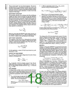
The DC current sample is obtained using the CS and CSG
pins connected to either a source sense resistor (RS) or the
RDS(ON) of the low-side MOSFET. For RDS(ON) sensing, RS =
RDS(ON) of the low-side MOSFET. In this case it is sometimes
helpful to adjust the current sense amplifier gain (A) to a lower
value in order to obtain the desired current limit. Adding ex-
ternal resistors RG in series with CS and CSG, the current
sense amplifier gain A becomes:
IR = 5µA/V x (VIN-VOUT) + 25µA
Current Limit
Proper selection of the RAMP capacitor (CRAMP) depends up-
on the value of the output inductor (L) and the current sense
resistor (RS). For proper current emulation, the DC sample
and hold value and the ramp amplitude must have the same
dependence on the load current. That is:
The LM25116 contains a current limit monitoring scheme to
protect the circuit from possible over-current conditions.
When set correctly, the emulated current sense signal is pro-
portional to the buck switch current with a scale factor deter-
mined by the current limit sense resistor. The emulated ramp
signal is applied to the current limit comparator. If the emu-
lated ramp signal exceeds 1.6V, the current cycle is termi-
nated (cycle-by-cycle current limiting). Since the ramp
amplitude is proportional to VIN - VOUT, if VOUT is shorted, there
is an immediate reduction in duty cycle. To further protect the
external switches during prolonged current limit conditions,
an internal counter counts clock pulses when in current limit.
When the counter detects 256 consecutive clock cycles, the
regulator enters a low power dissipation hiccup mode of cur-
rent limit. The regulator is shut down by momentarily pulling
UVLO low, and the soft-start capacitor discharged. The reg-
ulator is restarted with a full soft-start cycle once UVLO
charges back to 1.215V. This process is repeated until the
fault is removed. The hiccup off-time can be controlled by a
capacitor to ground on the UVLO pin. In applications with low
output inductance and high input voltage, the switch current
may overshoot due to the propagation delay of the current
limit comparator. If an overshoot should occur, the sample-
and-hold circuit will detect the excess recirculating current. If
the sample-and-hold DC level exceeds the internal current
limit threshold, the buck switch will be disabled and skip puls-
es until the current has decayed below the current limit thresh-
old. This approach prevents current runaway conditions due
to propagation delays or inductor saturation since the inductor
current is forced to decay following any current overshoot.
Where gm is the ramp generator transconductance (5µA/V)
and A is the current sense amplifier gain (10V/V). The ramp
capacitor should be located very close to the device and con-
nected directly to the pins of the IC (RAMP and AGND).
The difference between the average inductor current and the
DC value of the sampled inductor current can cause instability
for certain operating conditions. This instability is known as
sub-harmonic oscillation, which occurs when the inductor rip-
ple current does not return to its initial value by the start of
next switching cycle. Sub-harmonic oscillation is normally
characterized by observing alternating wide and narrow puls-
es at the switch node. Adding a fixed slope voltage ramp
(slope compensation) to the current sense signal prevents
this oscillation. The 25µA of offset current provided from the
emulated current source adds the optimal slope compensa-
tion to the ramp signal for a 5V output. For higher output
voltages, additional slope compensation may be required. In
these applications, the ramp capacitor can be decreased from
its nominal value to increase the ramp slope compensation.
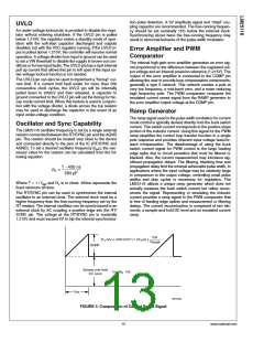
30015647
FIGURE 6. RDS(ON) Current Sensing without Diode
Emulation
www.national.com
14

 NSC [ National Semiconductor ]