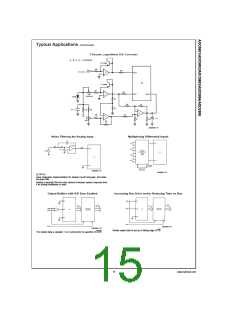
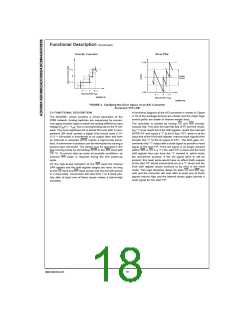
Functional Description (Continued)
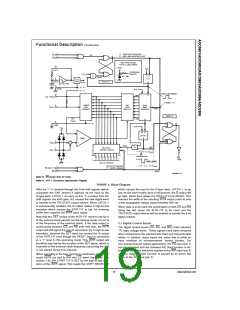
DS005671-13
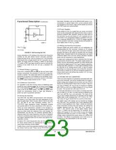
Note 13: CS shown twice for clarity.
=
Note 14: SAR Successive Approximation Register.
FIGURE 4. Block Diagram
After the “1” is clocked through the 8-bit shift register (which
completes the SAR search) it appears as the input to the
D-type latch, LATCH 1. As soon as this “1” is output from the
shift register, the AND gate, G2, causes the new digital word
to transfer to the TRI-STATE output latches. When LATCH 1
is subsequently enabled, the Q output makes a high-to-low
transition which causes the INTR F/F to set. An inverting
buffer then supplies the INTR input signal.
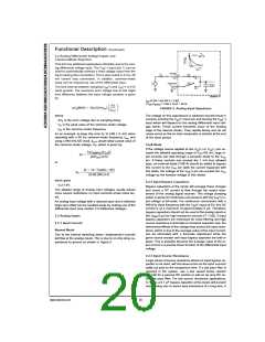
which causes the input to the D-type latch, LATCH 1, to go
low. As the latch enable input is still present, the Q output will
go high, which then allows the INTR F/F to be RESET. This
reduces the width of the resulting INTR output pulse to only
a few propagation delays (approximately 300 ns).
When data is to be read, the combination of both CS and RD
being low will cause the INTR F/F to be reset and the
TRI-STATE output latches will be enabled to provide the 8-bit
digital outputs.
Note that this SET control of the INTR F/F remains low for 8
of the external clock periods (as the internal clocks run at 1
⁄8
2.1 Digital Control Inputs
of the frequency of the external clock). If the data output is
continuously enabled (CS and RD both held low), the INTR
output will still signal the end of conversion (by a high-to-low
transition), because the SET input can control the Q output
of the INTR F/F even though the RESET input is constantly
at a “1” level in this operating mode. This INTR output will
therefore stay low for the duration of the SET signal, which is
8 periods of the external clock frequency (assuming the A/D
is not started during this interval).
The digital control inputs (CS, RD, and WR) meet standard
T2L logic voltage levels. These signals have been renamed
when compared to the standard A/D Start and Output Enable
labels. In addition, these inputs are active low to allow an
easy interface to microprocessor control busses. For
non-microprocessor based applications, the CS input (pin 1)
can be grounded and the standard A/D Start function is ob-
tained by an active low pulse applied at the WR input (pin 3)
and the Output Enable function is caused by an active low
pulse at the RD input (pin 2).
When operating in the free-running or continuous conversion
mode (INTR pin tied to WR and CS wired low — see also
section 2.8), the START F/F is SET by the high-to-low tran-
sition of the INTR signal. This resets the SHIFT REGISTER
19
www.national.com

 NSC [ National Semiconductor ]