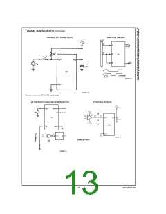
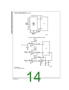
Typical Applications (Continued)
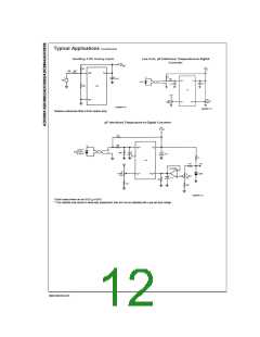
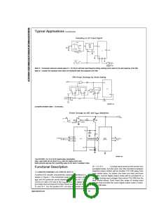
Sampling an AC Input Signal
DS005671-78
>
Note 11: Oversample whenever possible [keep fs 2f(−60)] to eliminate input frequency folding (aliasing) and to allow for the skirt response of the filter.
Note 12: Consider the amplitude errors which are introduced within the passband of the filter.
70% Power Savings by Clock Gating
DS005671-79
(Complete shutdown takes ≈ 30 seconds.)
Power Savings by A/D and VREF Shutdown
DS005671-80
*Use ADC0801, 02, 03 or 05 for lowest power consumption.
Note: Logic inputs can be driven to V
CC
with A/D supply at zero volts.
Buffer prevents data bus from overdriving output of A/D when in shutdown mode.
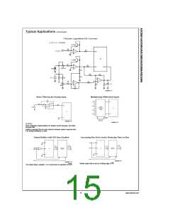
(A−1, A, A+1, . . . . ) analog inputs produce the correct out-
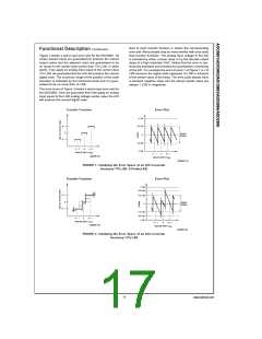
Functional Description
put digital codes, but also each riser (the transitions between
1
±
adjacent output codes) will be located
⁄2 LSB away from
1.0 UNDERSTANDING A/D ERROR SPECS
each center-value. As shown, the risers are ideal and have
A perfect A/D transfer characteristic (staircase waveform) is
shown in Figure 1. The horizontal scale is analog input volt-
age and the particular points labeled are in steps of 1 LSB
(19.53 mV with 2.5V tied to the VREF/2 pin). The digital out-
put codes that correspond to these inputs are shown as D−1,
D, and D+1. For the perfect A/D, not only will center-value
no width. Correct digital output codes will be provided for a
1
±
range of analog input voltages that extend
⁄2 LSB from the
ideal center-values. Each tread (the range of analog input
voltage that provides the same digital output code) is there-
fore 1 LSB wide.
www.national.com
16

 NSC [ National Semiconductor ]