Functional Description (Continued)
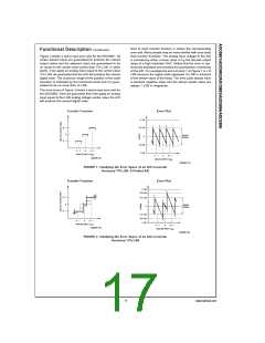
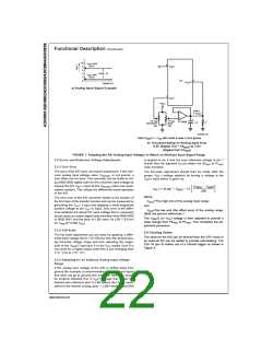
Transfer Function
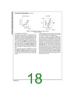
Error Plot
DS005671-85
DS005671-86
FIGURE 3. Clarifying the Error Specs of an A/D Converter
1
=
±
Accuracy
⁄2 LSB
2.0 FUNCTIONAL DESCRIPTION
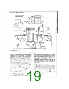
A functional diagram of the A/D converter is shown in Figure
4. All of the package pinouts are shown and the major logic
control paths are drawn in heavier weight lines.
The ADC0801 series contains a circuit equivalent of the
256R network. Analog switches are sequenced by succes-
sive approximation logic to match the analog difference input
voltage [VIN(+) − VIN(−)] to a corresponding tap on the R net-
work. The most significant bit is tested first and after 8 com-
parisons (64 clock cycles) a digital 8-bit binary code (1111
The converter is started by having CS and WR simulta-
neously low. This sets the start flip-flop (F/F) and the result-
ing “1” level resets the 8-bit shift register, resets the Interrupt
(INTR) F/F and inputs a “1” to the D flop, F/F1, which is at the
input end of the 8-bit shift register. Internal clock signals then
transfer this “1” to the Q output of F/F1. The AND gate, G1,
combines this “1” output with a clock signal to provide a reset
signal to the start F/F. If the set signal is no longer present
(either WR or CS is a “1”) the start F/F is reset and the 8-bit
shift register then can have the “1” clocked in, which starts
the conversion process. If the set signal were to still be
present, this reset pulse would have no effect (both outputs
of the start F/F would momentarily be at a “1” level) and the
8-bit shift register would continue to be held in the reset
mode. This logic therefore allows for wide CS and WR sig-
nals and the converter will start after at least one of these
signals returns high and the internal clocks again provide a
reset signal for the start F/F.
=
1111 full-scale) is transferred to an output latch and then
an interrupt is asserted (INTR makes a high-to-low transi-
tion). A conversion in process can be interrupted by issuing a
second start command. The device may be operated in the
free-running mode by connecting INTR to the WR input with
=
CS 0. To ensure start-up under all possible conditions, an
external WR pulse is required during the first power-up
cycle.
On the high-to-low transition of the WR input the internal
SAR latches and the shift register stages are reset. As long
as the CS input and WR input remain low, the A/D will remain
in a reset state. Conversion will start from 1 to 8 clock peri-
ods after at least one of these inputs makes a low-to-high
transition.
www.national.com
18

 NSC [ National Semiconductor ]