Functional Description (Continued)
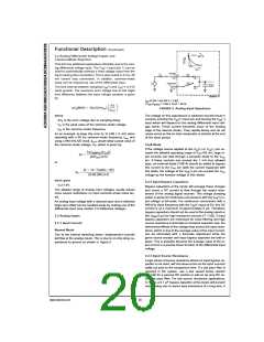
DS005671-87
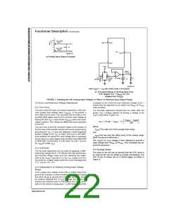
a) Analog Input Signal Example
DS005671-88
*
Add if V
REF
/2 ≤ 1 V with LM358 to draw 3 mA to ground.
DC
b) Accommodating an Analog Input from
=
0.5V (Digital Out 00HEX) to 3.5V
=
(Digital Out FFHEX
)
FIGURE 7. Adapting the A/D Analog Input Voltages to Match an Arbitrary Input Signal Range
2.5 Errors and Reference Voltage Adjustments
is applied to pin 6 and the zero reference voltage at pin 7
should then be adjusted to just obtain the 00HEX to 01HEX
code transition.
2.5.1 Zero Error
The zero of the A/D does not require adjustment. If the mini-
mum analog input voltage value, VIN(MIN), is not ground, a
zero offset can be done. The converter can be made to out-
put 0000 0000 digital code for this minimum input voltage by
biasing the A/D VIN(−) input at this VIN(MIN) value (see Appli-
cations section). This utilizes the differential mode operation
of the A/D.
The full-scale adjustment should then be made (with the
proper VIN(−) voltage applied) by forcing a voltage to the
V
IN(+) input which is given by:
where:
The zero error of the A/D converter relates to the location of
the first riser of the transfer function and can be measured by
grounding the VIN (−) input and applying a small magnitude
positive voltage to the VIN (+) input. Zero error is the differ-
ence between the actual DC input voltage that is necessary
=
VMAX The high end of the analog input range
and
=
VMIN the low end (the offset zero) of the analog range.
(Both are ground referenced.)
to just cause an output digital code transition from 0000 0000
The VREF/2 (or VCC) voltage is then adjusted to provide a
code change from FEHEX to FFHEX. This completes the ad-
justment procedure.
1
to 0000 0001 and the ideal
⁄2
LSB value (1⁄
LSB 9.8 mV
=
2
=
for VREF/2 2.500 VDC).
2.5.2 Full-Scale
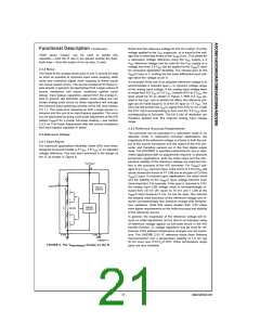
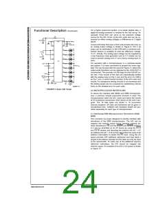
2.6 Clocking Option
The full-scale adjustment can be made by applying a differ-
ential input voltage that is 11⁄
LSB less than the desired ana-
log full-scale voltage range and then adjusting the magni-
tude of the VREF/2 input (pin 9 or the VCC supply if pin 9 is
not used) for a digital output code that is just changing from
1111 1110 to 1111 1111.
The clock for the A/D can be derived from the CPU clock or
an external RC can be added to provide self-clocking. The
CLK IN (pin 4) makes use of a Schmitt trigger as shown in
Figure 8.
2
2.5.3 Adjusting for an Arbitrary Analog Input Voltage
Range
If the analog zero voltage of the A/D is shifted away from
ground (for example, to accommodate an analog input signal
that does not go to ground) this new zero reference should
be properly adjusted first. A VIN(+) voltage that equals this
desired zero reference plus 1
⁄ LSB (where the LSB is calcu-
2
=
lated for the desired analog span, 1 LSB analog span/256)
www.national.com
22

 NSC [ National Semiconductor ]