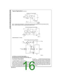
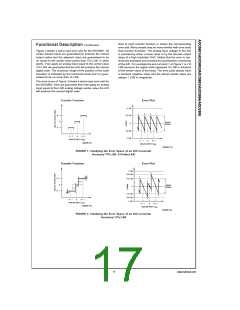
Next to each transfer function is shown the corresponding
error plot. Many people may be more familiar with error plots
than transfer functions. The analog input voltage to the A/D
is provided by either a linear ramp or by the discrete output
steps of a high resolution DAC. Notice that the error is con-
tinuously displayed and includes the quantization uncertainty
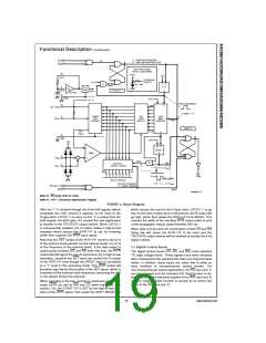
Functional Description (Continued)
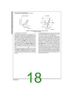
Figure 2 shows a worst case error plot for the ADC0801. All
center-valued inputs are guaranteed to produce the correct
output codes and the adjacent risers are guaranteed to be
1
±
no closer to the center-value points than
⁄4 LSB. In other
words, if we apply an analog input equal to the center-value
of the A/D. For example the error at point 1 of Figure 1 is +1⁄
2
1
1
±
⁄4
LSB, we guarantee that the A/D will produce the correct
LSB because the digital code appeared
⁄2 LSB in advance
digital code. The maximum range of the position of the code
of the center-value of the tread. The error plots always have
a constant negative slope and the abrupt upside steps are
always 1 LSB in magnitude.
transition is indicated by the horizontal arrow and it is guar-
1
anteed to be no more than
⁄2 LSB.
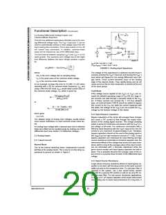
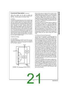
The error curve of Figure 3 shows a worst case error plot for
the ADC0802. Here we guarantee that if we apply an analog
input equal to the LSB analog voltage center-value the A/D
will produce the correct digital code.
Transfer Function
Error Plot
DS005671-81
DS005671-82
FIGURE 1. Clarifying the Error Specs of an A/D Converter
=
±
Accuracy 0 LSB: A Perfect A/D
Transfer Function
Error Plot
DS005671-83
DS005671-84
FIGURE 2. Clarifying the Error Specs of an A/D Converter
1
=
±
Accuracy
⁄4 LSB
17
www.national.com

 NSC [ National Semiconductor ]