(low power Schottky such as the DM74LS240 series is rec-
ommended) or special higher drive current products which
are designed as bus drivers. High current bipolar bus drivers
with PNP inputs are recommended.
Functional Description (Continued)
2.10 Power Supplies
Noise spikes on the VCC supply line can cause conversion
errors as the comparator will respond to this noise. A low in-
ductance tantalum filter capacitor should be used close to
the converter VCC pin and values of 1 µF or greater are rec-
ommended. If an unregulated voltage is available in the sys-
tem, a separate LM340LAZ-5.0, TO-92, 5V voltage regulator
for the converter (and other analog circuitry) will greatly re-
duce digital noise on the VCC supply.
DS005671-17
2.11 Wiring and Hook-Up Precautions
Standard digital wire wrap sockets are not satisfactory for
breadboarding this A/D converter. Sockets on PC boards
can be used and all logic signal wires and leads should be
grouped and kept as far away as possible from the analog
signal leads. Exposed leads to the analog inputs can cause
undesired digital noise and hum pickup, therefore shielded
leads may be necessary in many applications.
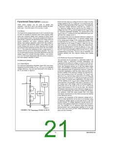
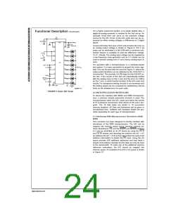
FIGURE 8. Self-Clocking the A/D
Heavy capacitive or DC loading of the clock R pin should be
avoided as this will disturb normal converter operation.
Loads less than 50 pF, such as driving up to 7 A/D converter
clock inputs from a single clock R pin of 1 converter, are al-
lowed. For larger clock line loading, a CMOS or low power
TTL buffer or PNP input logic should be used to minimize the
loading on the clock R pin (do not use a standard TTL
buffer).
A single point analog ground that is separate from the logic
ground points should be used. The power supply bypass ca-
pacitor and the self-clocking capacitor (if used) should both
be returned to digital ground. Any VREF/2 bypass capacitors,
analog input filter capacitors, or input signal shielding should
be returned to the analog ground point. A test for proper
grounding is to measure the zero error of the A/D converter.
2.7 Restart During a Conversion
1
Zero errors in excess of
⁄4 LSB can usually be traced to im-
If the A/D is restarted (CS and WR go low and return high)
during a conversion, the converter is reset and a new con-
version is started. The output data latch is not updated if the
conversion in process is not allowed to be completed, there-
fore the data of the previous conversion remains in this latch.
The INTR output simply remains at the “1” level.
proper board layout and wiring (see section 2.5.1 for mea-
suring the zero error).
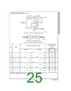
3.0 TESTING THE A/D CONVERTER
There are many degrees of complexity associated with test-
ing an A/D converter. One of the simplest tests is to apply a
known analog input voltage to the converter and use LEDs to
display the resulting digital output code as shown in Figure 9.
2.8 Continuous Conversions
For operation in the free-running mode an initializing pulse
should be used, following power-up, to ensure circuit opera-
tion. In this application, the CS input is grounded and the WR
input is tied to the INTR output. This WR and INTR node
For ease of testing, the VREF/2 (pin 9) should be supplied
with 2.560 VDC and a VCC supply voltage of 5.12 VDC should
be used. This provides an LSB value of 20 mV.
If a full-scale adjustment is to be made, an analog input volt-
should be momentarily forced to logic low following
power-up cycle to guarantee operation.
a
age of 5.090 VDC (5.120–11⁄
V
V
2
LSB) should be applied to the
IN(+) pin with the VIN(−) pin grounded. The value of the
REF/2 input voltage should then be adjusted until the digital
2.9 Driving the Data Bus
output code is just changing from 1111 1110 to 1111 1111.
This value of VREF/2 should then be used for all the tests.
This MOS A/D, like MOS microprocessors and memories,
will require a bus driver when the total capacitance of the
data bus gets large. Other circuitry, which is tied to the data
bus, will add to the total capacitive loading, even in
TRI-STATE (high impedance mode). Backplane bussing
also greatly adds to the stray capacitance of the data bus.
The digital output LED display can be decoded by dividing
the 8 bits into 2 hex characters, the 4 most significant (MS)
and the 4 least significant (LS). Table 1 shows the fractional
binary equivalent of these two 4-bit groups. By adding the
voltages obtained from the “VMS” and “VLS” columns in
Table 1, the nominal value of the digital display (when
There are some alternatives available to the designer to
handle this problem. Basically, the capacitive loading of the
data bus slows down the response time, even though DC
specifications are still met. For systems operating with a
relatively slow CPU clock frequency, more time is available
in which to establish proper logic levels on the bus and there-
fore higher capacitive loads can be driven (see typical char-
acteristics curves).
=
V
REF/2 2.560V) can be determined. For example, for an
output LED display of 1011 0110 or B6 (in hex), the voltage
values from the table are 3.520 + 0.120 or 3.640 VDC. These
voltage values represent the center-values of a perfect A/D
converter. The effects of quantization error have to be ac-
counted for in the interpretation of the test results.
At higher CPU clock frequencies time can be extended for
I/O reads (and/or writes) by inserting wait states (8080) or
using clock extending circuits (6800).
Finally, if time is short and capacitive loading is high, external
bus drivers must be used. These can be TRI-STATE buffers
23
www.national.com

 NSC [ National Semiconductor ]