PBSS8110X
NXP Semiconductors
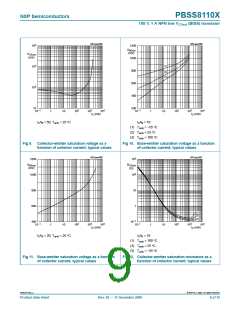
100 V, 1 A NPN low VCEsat (BISS) transistor
5. Limiting values
Table 5.
Limiting values
In accordance with the Absolute Maximum Rating System (IEC 60134).
Symbol
VCBO
VCEO
VEBO
IC
Parameter
Conditions
Min
Max
120
100
5
Unit
V
collector-base voltage
open emitter
-
-
-
-
-
collector-emitter voltage open base
V
emitter-base voltage
collector current (DC)
peak collector current
open collector
V
1
A
ICM
single pulse;
3
A
tp ≤ 1 ms
IB
base current (DC)
-
300
0.55
1.4
mA
W
[1]
[2]
[3]
Ptot
total power dissipation
Tamb ≤ 25 °C
-
-
W
-
2.0
W
Tj
junction temperature
ambient temperature
storage temperature
-
150
+150
+150
°C
°C
°C
Tamb
Tstg
−65
−65
[1] Device mounted on an FR4 Printed-Circuit Board (PCB), single-sided copper, tin-plated and standard
footprint.
[2] Device mounted on an FR4 PCB, single-sided copper, tin-plated, mounting pad for collector 6cm2.
[3] Device mounted on a ceramic PCB, Al2O3, standard footprint.
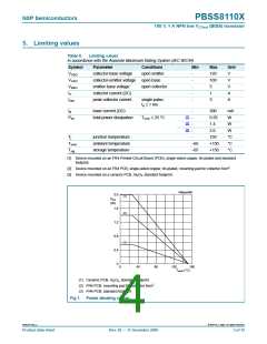
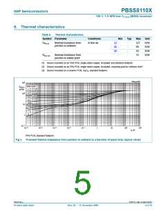
006aaa408
2.0
(1)
P
tot
(W)
1.6
(2)
1.2
0.8
0.4
0
(3)
0
40
80
120
160
(°C)
T
amb
(1) Ceramic PCB, Al2O3, standard footprint
(2) FR4 PCB; mounting pad for collector 6cm2
(3) FR4 PCB; standard footprint
Fig 1. Power derating curves
PBSS8110X_2
© NXP B.V. 2009. All rights reserved.
Product data sheet
Rev. 02 — 11 December 2009
3 of 15

 NEXPERIA [ Nexperia ]