PBSS8110X
NXP Semiconductors
100 V, 1 A NPN low VCEsat (BISS) transistor
8. Test information
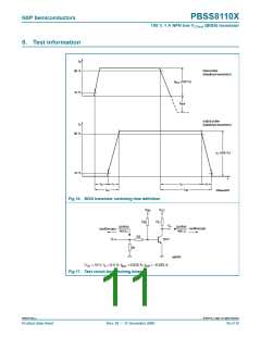
I
B
input pulse
90 %
(idealized waveform)
I
(100 %)
Bon
10 %
I
Boff
output pulse
(idealized waveform)
I
C
90 %
I
(100 %)
C
10 %
t
t
t
f
t
t
r
s
d
t
t
off
on
006aaa003
Fig 16. BISS transistor switching time definition
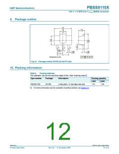
V
V
CC
BB
R
R
C
B
V
o
(probe)
(probe)
oscilloscope
oscilloscope
450 Ω
450 Ω
R2
V
I
DUT
R1
mlb826
VCC = 10 V; IC = 0.5 A; IBon = 0.025 A; IBoff = −0.025 A
Fig 17. Test circuit for switching times
PBSS8110X_2
© NXP B.V. 2009. All rights reserved.
Product data sheet
Rev. 02 — 11 December 2009
10 of 15

 NEXPERIA [ Nexperia ]