Nexperia
PBSS4260PANPS
60 V, 2 A NPN/PNP low VCEsat (BISS) double transistor
11. Test information
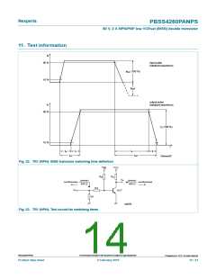
I
B
input pulse
90 %
(idealized waveform)
I
(100 %)
Bon
10 %
I
Boff
output pulse
(idealized waveform)
I
C
90 %
I
(100 %)
C
10 %
t
t
t
f
t
t
r
s
d
t
t
off
on
006aaa003
Fig. 22. TR1 (NPN): BISS transistor switching time definition
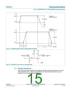
V
V
CC
BB
R
B
R
C
V
o
(probe)
450 Ω
(probe)
450 Ω
oscilloscope
oscilloscope
R2
V
I
DUT
R1
mlb826
Fig. 23. TR1 (NPN): Test circuit for switching times
©
PBSS4260PANPS
All information provided in this document is subject to legal disclaimers.
Nexperia B.V. 2017. All rights reserved
Product data sheet
4 February 2016
14 / 21

 NEXPERIA [ Nexperia ]