Nexperia
PBSS4260PANPS
60 V, 2 A NPN/PNP low VCEsat (BISS) double transistor
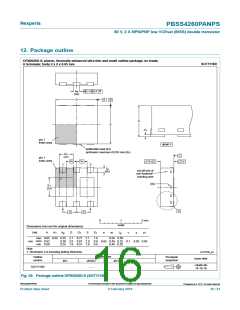
12. Package outline
DFN2020D-6: plastic, thermally enhanced ultra thin and small outline package; no leads;
6 terminals; body 2 x 2 x 0.65 mm
SOT1118D
b
v
A B
p
(6x)
D
A
B
A
E
A
1
pin 1
index area
detail X
solderable lead end
protrusion maximum 0.035 mm (6x)
D
1
C
(2x)
pin 1
index area
e
e
1
y
C
1
y
1
3
1
L
(6x)
p
cut-off end of
non-fuctional
bonding wire
(8x)
E
1
(2x)
4
6
X
e
e
0
1
2 mm
scale
Dimensions (mm are the original dimensions)
Unit
max 0.65 0.04 0.35 2.1 0.77 2.1
A
A
b
D
D
1
E
E
e
e
1
L
p
v
y
y
1
1
p
1
1.0
0.9 0.65 0.49 0.25 0.1 0.05 0.05
0.8 0.44 0.20
0.54 0.30
nom
mm
0.62
0.30 2.0 0.67 2.0
0.25 1.9 0.57 1.9
min 0.59
Note
1. Dimension A is including plating thickness.
sot1118d_po
References
Outline
version
IEC
European
projection
Issue date
JEDEC
- - -
JEITA
14-07-16
14-10-16
SOT1118D
Fig. 26. Package outline DFN2020D-6 (SOT1118D)
©
PBSS4260PANPS
All information provided in this document is subject to legal disclaimers.
Nexperia B.V. 2017. All rights reserved
Product data sheet
4 February 2016
16 / 21

 NEXPERIA [ Nexperia ]