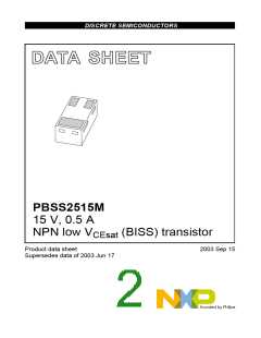
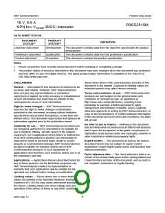
NXP Semiconductors
Product data sheet
15 V, 0.5 A
NPN low VCEsat (BISS) transistor
PBSS2515M
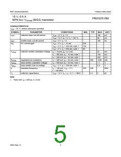
LIMITING VALUES
In accordance with the Absolute Maximum Rating System (IEC 60134).
SYMBOL
PARAMETER
collector-base voltage
CONDITIONS
open emitter
MIN.
MAX.
15
UNIT
VCBO
VCEO
VEBO
IC
−
−
−
−
−
−
−
−
V
V
V
collector-emitter voltage
emitter-base voltage
collector current (DC)
peak collector current
peak base current
open base
15
open collector
notes 1 and 2
6
500
1
mA
A
ICM
IBM
100
250
430
+150
150
+150
mA
mW
mW
°C
Ptot
total power dissipation
Tamb ≤ 25 °C; notes 1 and 2
Tamb ≤ 25 °C; note 1 and 3
Tstg
Tj
storage temperature
−65
−
junction temperature
°C
Tamb
operating ambient temperature
−65
°C
Notes
1. Refer to SOT883 standard mounting conditions.
2. Device mounted on an FR4 printed-circuit board, single-sided copper, tinplated, standard footprint, with 60 μm
copper strip line.
3. Device mounted on a printed-circuit board, single-sided copper, tinplated, mounting pad for collector 1 cm2.
THERMAL CHARACTERISTICS
SYMBOL
PARAMETER
CONDITIONS
VALUE
UNIT
Rth j-a
thermal resistance from junction to
ambient
in free air; notes 1 and 2
500
290
K/W
K/W
in free air; notes 1, 3 and 4
Notes
1. Refer to SOT883 standard mounting conditions.
2. Device mounted on an FR4 printed-circuit board, single-sided copper, tinplated, standard footprint, with 60 μm
copper strip line.
3. Device mounted on a printed-circuit board, single-sided copper, tinplated, mounting pad for collector 1 cm2.
4. Operated under pulsed conditions: duty cycle δ ≤ 20%, pulse width tp ≤ 30 ms.
Soldering
Reflow soldering is the only recommended soldering method.
2003 Sep 15
3

 NEXPERIA [ Nexperia ]