CHAPTER 1 INTRODUCTION
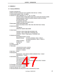
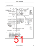
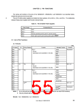
1.4.5 Function block configuration (V850ES/KJ1)
(1) Internal block diagram
ROM
CPU
NMI
INTC
16-bit
timer/event
counter: 6 ch
Instruction
queue
INTP0 to INTP6
PC
Note 1
TI000, TI001, TI010, TI011,
TI020, TI021, TI030, TI031,
TI040, TI041, TI050, TI051
HLDRQ
HLDAK
ASTB
RD
32-bit barrel
shifter
Multiplier
16 × 16→32
RAM
6 KB
TO00 to TO05
System
registers
WAIT
BCU
WR0, WR1
CS0 to CS3
A0 to A23
ALU
8-bit
timer/event
counter: 2 ch
TI50, TI51
General-purpose
registers
32 bits × 32
TO50, TO51
ROM
AD0 to AD15
correction
8-bit timer H:
TOH0, TOH1
2 ch
SIO
CLKOUT
Ports
D/A
A/D
SO00 to SO02
SI00 to SI02
SCK00 to SCK02
X1
converter
converter
CSI0: 3 ch
X2
CG
XT1
XT2
RESET
SOA0, SOA1
SIA0, SIA1
SCKA0, SCKA1
CSIA: 2 ch
SDA0, SDA1Note 2
SCL0, SCL1Note 2
I2CNote 3
: 2 ch
Regulator
V
DD
TXD0 to TXD2
RXD0 to RXD2
ASCK0
ICNote 3
BVDD
BVSS
EVDD
EVSS
UART: 3 ch
Key interrupt
Watchdog
timer
KR0 to KR7
function
Note 4
V
V
PP
SS
RTP00 to RTP05,
RTP10 to RTP15
Watch timer
RTP: 2 ch
Notes 1. µPD703216, 703216Y:
µPD703217, 703217Y:
96 KB (mask ROM)
128 KB (mask ROM)
µPD70F3217, 70F3217Y: 128 KB (flash memory)
2. Only for the µPD703216Y, 703217Y, 70F3217Y
3. Only for the µPD703216, 703216Y, 703217, and 703217Y
4. Only for the µPD70F3217 and 70F3217Y
User’s Manual U15862EJ3V0UD
51

 NEC [ NEC ]