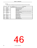
CHAPTER 1 INTRODUCTION
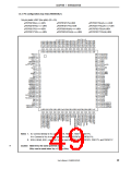
Pin Identification (V850ES/KJ1)
A0 to A23:
AD0 to AD15:
ANI0 to ANI15:
ANO0, ANO1:
ASCK0:
Address bus
PDL0 to PDL15:
Port DL
Address/data bus
Analog input
RD:
Read strobe
Regulator control
Reset
REGC:
Analog output
Asynchronous serial clock
Address strobe
Analog reference voltage
Ground for analog
Power supply for bus interface
Ground for bus interface
Clock output
RESET:
RTP00 to RTP05,
RTP10 to RTP15:
RXD0 to RXD2:
SCK00 to SCK02,
SCKA0, SCKA1:
SCL0, SCL1:
SDA0, SDA1:
SI00 to SI02,
SIA0, SIA1:
SO00 to SO02,
SOA0, SOA1:
TI000, TI001,
TI010, TI011,
TI020, TI021,
TI030, TI031,
TI040, TI041,
TI050, TI051,
TI50, TI51:
TO00 to TO05,
TO50, TO51,
TOH0, TOH1:
TXD0 to TXD2:
VDD:
ASTB:
Real-time output port
Receive data
AVREF0, AVREF1:
AVSS:
BVDD:
Serial clock
Serial clock
Serial data
BVSS:
CLKOUT:
CS0 to CS3:
EVDD:
Chip select
Power supply for port
Ground for port
Hold acknowledge
Hold request
Internally connected
Interrupt request from peripherals
Key return
Serial input
EVSS:
HLDAK:
Serial output
HLDRQ:
IC:
INTP0 to INTP6:
KR0 to KR7:
NMI:
Non-maskable interrupt request
Port 0
P00 to P06:
P10, P11:
Port 1
Timer input
P30 to P39:
P40 to P42:
P50 to P55:
P60 to P615:
P70 to P715:
P80, P81:
Port 3
Port 4
Port 5
Timer output
Port 6
Transmit data
Port 7
Power supply
Port 8
VPP:
Programming power supply
Ground
P90 to P915:
PCD0 to PCD3:
PCM0 to PCM5:
PCS0 to PCS7:
PCT0 to PCT7:
PDH0 to PDH7:
Port 9
VSS:
Port CD
WAIT:
Wait
Port CM
WR0:
Lower byte write strobe
Upper byte write strobe
Crystal for main clock
Crystal for subclock
Port CS
WR1:
Port CT
X1, X2:
Port DH
XT1, XT2:
User’s Manual U15862EJ3V0UD
50

 NEC [ NEC ]