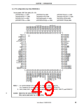
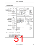
CHAPTER 1 INTRODUCTION
(i) Watchdog timer
Two watchdog timer channels are provided on chip to detect program loops and system abnormalities.
Watchdog timer 1 can be used as an interval timer. When used as a watchdog timer, it generates a non-
maskable interrupt request signal (INTWDT1) or system reset signal (WDTRES1) after an overflow
occurs. When used as an interval timer, it generates a maskable interrupt request signal (INTWDTM1)
after an overflow occurs.
Watchdog timer 2 operates by default following reset release.
It generates a non-maskable interrupt request signal (INTWDT2) or system reset signal (WDTRES2) after
an overflow occurs.
(j) Serial interface (SIO)
The V850ES/KJ1 includes four kinds of serial interfaces: an asynchronous serial interface (UARTn), a
clocked serial interface (CSI0n), a clocked serial interface (with an automatic transmit/receive function)
(CSIAm), and an I2C bus interface (I2Cm). The µPD703216, 703217, and 70F3217 can simultaneously
use up to eight channels, and the µPD703216Y, 703217Y, and 70F3217Y up to nine channels.
For UARTn, data is transferred via the TXDn and RXDn pins.
For CSI0n, data is transferred via the SO0n, SI0n, and SCK0n pins.
For CSIAm, data is transferred via the SOAm, SIAm, and SCKAm pins.
For I2Cm, data is transferred via the SDAm and SCLm pins.
I2Cm is provided only for the µPD703216Y, 703217Y, and 70F3217Y.
For UART, a dedicated baud rate generator is provided on chip.
Remark n = 0 to 2
m = 0, 1
(k) A/D converter
This high-speed, high-resolution 10-bit A/D converter includes 16 analog input pins. Conversion is
performed using the successive approximation method.
(l) D/A converter
Two 8-bit resolution D/A converter channels are included on chip. It uses the R-2R ladder method.
(m) ROM correction
This function is used to replace part of a program in the mask ROM with that contained in the internal
RAM. Up to four correction addresses can be specified.
(n) Key interrupt function
A key interrupt request signal (INTKR) can be generated by inputting a falling edge to the eight key input
pins.
(o) Real-time output function
This function transfers 6-bit data set beforehand to output latches upon occurrence of an external trigger
signal or a timer compare register match signal.
For the V850ES/KJ1, a 2-channel 6-bit data real-time output function is provided on chip.
User’s Manual U15862EJ3V0UD
53

 NEC [ NEC ]