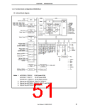
CHAPTER 2 PIN FUNCTIONS
The names and functions of the pins of the V850ES/KF1, V850ES/KG1, and V850ES/KJ1 are described below,
divided into port pins and non-port pins.
The pin I/O buffer power supplies are divided into three systems; AVREF0/AVREF1, BVDD, and EVDD. The relationship
between these power supplies and the pins is shown below.
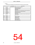
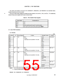
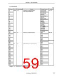
Table 2-1. Pin I/O Buffer Power Supplies
Power Supply
AVREF0
Corresponding Pin
Port 7
Port 1
AVREF1
BVDD
Port CD, port CM, port CS, port CT, port DH, port DL
Port 0, port 3, port 4, port 5, port 6, port 8, port 9, RESET
EVDD
2.1 List of Pin Functions
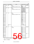
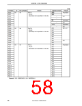
(1) Port pins
(1/4)
Products
Pin Name
P00
I/O
I/O
Pull-up Resistor
Yes
Function
Alternate Function
Port 0
TOH0
TOH1
NMI
All products
I/O port
P01
Input/output can be specified in 1-bit units.
P02
P03
INTP0
INTP1
INTP2
INTP3
ANO0
P04
P05
P06
P10
I/O
I/O
Yes
Yes
Port 1
KG1, KJ1
I/O port
P11
ANO1
Input/output can be specified in 1-bit units.
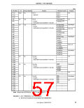
P30
P31
P32
P33
P34
P35
P36
P37
P38
P39
Port 3
TXD0
All products
I/O port
RXD0
Input/output can be specified in 1-bit units.
ASCK0
TI000/TO00
TI001
TI010/TO01
–
NoNote 1
KG1, KJ1
–
SDA0Note 2
SCL0Note 2
All products
Notes 1. An on-chip pull-up resistor can be provided by a mask option (only for the mask ROM versions).
2. Only for products with an I2C bus
Remark KG1: V850ES/KG1, KJ1: V850ES/KJ1
55
User’s Manual U15862EJ3V0UD

 NEC [ NEC ]