µPD703100A-33, 703100A-40, 703101A-33, 703102A-33
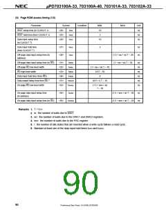
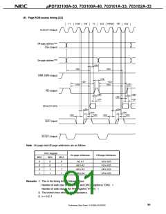
(5) Page ROM access timing (2/2)
T1
TDW
TW
T2
TO1 TPRW
TW
TO2
CLKOUT (Output)
Off-page address Note
CSn (Output)
On-page address Note
UWR, LWR (Output)
RD (Output)
<26>
<30>
<31>
<54>
<33>
<53>
<55>
<32>
<37>
<36>
<27>
<36>
<27>
<26>
<25>
D0 to D15 (I/O)
WAIT (Input)
<25>
<24>
<24>
<25>
<24>
<25>
<24>
BCYST (Output)
Note On-page and off-page addresses are as follows.
PRC Register
On-page Addresses
Off-page Addresses
MA5
MA4
MA3
0
0
0
1
0
0
1
1
0
1
1
1
A0, A1
A0 to A2
A0 to A3
A0 to A4
A2 to A23
A3 to A23
A4 to A23
A5 to A23
Remarks 1. This is the timing for the following case.
Number of waits due to the DWC1 and DWC2 registers (TDW): 1
Number of waits due to the PRC register (TPRW): 1
2. The broken lines indicate high impedance.
3. n = 0 to 7
91
Preliminary Data Sheet U14168EJ2V0DS00

 NEC [ NEC ]