µPD703100A-33, 703100A-40, 703101A-33, 703102A-33
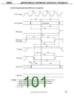
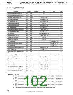
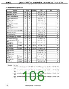
(e) Read timing (EDO DRAM) (1/3)
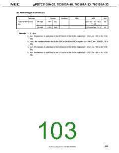
Parameter
Symbol
<26>
Condition
MIN.
10
MAX.
Unit
ns
ns
ns
ns
ns
ns
ns
ns
ns
ns
ns
ns
ns
ns
ns
ns
ns
ns
ns
ns
Data input setup time (to CLKOUT ↑)
Data input hold time (from CLKOUT ↑)
Data output delay time from OE ↑
Row address setup time
tSKID
tHKID
tDRDOD
tASR
tRAH
tASC
tCAH
tRP
<27>
<37>
<56>
<57>
<58>
<59>
<61>
<64>
<66>
<67>
<68>
<69>
<70>
<73>
<74>
<75>
<76>
<77>
<78>
2
(0.5 + i) T – 10
(0.5 + wRP) T – 10
(0.5 + wRH) T – 10
0.5T – 10
Row address hold time
Column address setup time
Column address hold time
RAS precharge time
(0.5 + wDA) T – 10
(0.5 + wRP) T – 5
(2 + wCP + wDA) T – 10
(1 + wRP) T – 10
Column address read time (from RAS
CAS-RAS precharge time
CAS hold time
↑
)
tRAL
tCRP
tCSH
tRCS
tRRH
tRCH
tRAC
tAA
(1.5 + wRH + wDA) T – 10
WE setup time (to CAS ↓)
WE hold time (from RAS ↑)
WE hold time (from CAS ↑)
RAS access time
(2 + wRP + wRH) T – 10
0.5T – 10
1.5T – 10
(2 + wRH + wDA) T – 20
Access time from column address
CAS access time
(1.5 + wDA) T – 20
(1 + wDA) T – 20
tCAC
tRAD
tRCD
tOEZ
Column address delay time from RAS
RAS-CAS delay time
(0.5 + wRH) T – 10
(1 + wRH) T – 10
0
Output buffer turn-off delay time (from
OE)
Access time from CAS precharge
CAS precharge time
<80>
<81>
<83>
<93>
<94>
<95>
<96>
<97>
<98>
tACP
tCP
tRHCP
tHPC
(1.5 + wCP + wDA
)
T – 20
ns
ns
ns
ns
ns
ns
ns
ns
ns
(0.5 + wCP) T – 5
(2 + wCP + wDA) T – 10
(1 + wDA + wCP) T – 10
RAS hold time for CAS precharge
Read cycle time
RAS pulse width
tRASP
tHCAS
tOCH1
tOCH2
tDHC
(2.5 + wRH + wDA) T – 10
CAS pulse width
(0.5 + wDA) T – 10
(2 + wRH + wDA) T – 10
(0.5 + wDA) T – 10
0
CAS hold time from OE
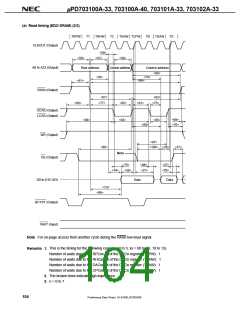
Off-page
On-page
Data input hold time (from CAS ↓)
Remarks 1. T = tCYK
2. wRP: the number of waits due to the RPCxx bit of the DRCn register (n = 0 to 3, xx = 00 to 03, 10 to
13).
3. wRH: the number of waits due to the RHCxx bit of the DRCn register (n = 0 to 3, xx = 00 to 03, 10 to
13).
4. wDA: the number of waits due to the DACxx bit of the DRCn register (n = 0 to 3, xx = 00 to 03, 10 to
13).
5. wCP: the number of waits due to the CPCxx bit of the DRCn register (n = 0 to 3, xx = 00 to 03, 10 to
13).
6. i: the number of idle states that are inserted when a write cycle follows a read cycle.
102
Preliminary Data Sheet U14168EJ2V0DS00

 NEC [ NEC ]