DDR3(L) 4Gb SDRAM
NT5CB(C)512M8DN / NT5CB(C)256M16DP
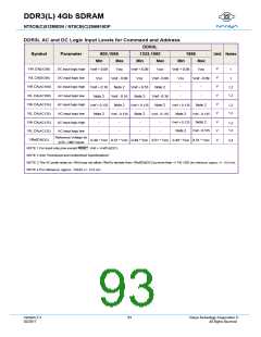
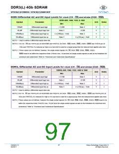
DDR3L AC and DC Logic Input Levels for Command and Address
DDR3L
Symbol
Parameter
800,1066
1333,1600
1866
Unit Notes
Min
Max
Min
Max
Min
Max
V
1
VIH.CA(DC90)
VIL.CA(DC90)
VIH.CA(AC160)
VIL.CA(AC160)
VIH.CA(AC135)
VIL.CA(AC135)
VIH.CA(AC125)
VIL.CA(AC125)
VRefCA(DC)
DC input logic high
DC input logic low
AC input logic high
AC input logic low
AC input logic high
AC input logic low
AC input logic high
AC input logic low
Vref + 0.09
VSS
VDD
Vref + 0.09
VSS
VDD
Vref + 0.09
VDD
V
1
Vref - 0.09
Note 2
Vref - 0.09
Note 2
VSS
Vref - 0.09
-
V
-
Vref + 0.16
Note 2
Vref + 0.16
Note 2
1,2
V
V
V
V
V
1,2
-
-
Vref - 0.16
Note 2
Vref - 0.16
Note 2
Vref + 0.135
Vref + 0.135
Vref + 0.135
Note 2
1,2
1,2
Note 2
Vref - 0.135
Note 2
Vref - 0.135
Note 2
Vref - 0.135
Note 2
Vref + 0.125
-
-
-
-
-
-
-
-
1,2
1,2
Note 2
Vref - 0.125
Reference Voltage for
ADD, CMD inputs
0.49 * VDD 0.51 * VDD 0.49 * VDD 0.51 * VDD 0.49 * VDD 0.51 * VDD
V
3,4
NOTE 1 For input only pins except REET. Vref = VrefCA(DC).
NOTE 2 See “Overshoot and Undershoot Specifications”
NOTE 3 The AC peak noise on VRef may not allow VRef to deviate from VRefDQ(DC) by more than +/-1% VDD (for reference: approx. +/- 13.5 mV).
NOTE 4 For reference: approx. VDD/2 +/- 13.5 mV
Version 2.3
02/2017
93
Nanya Technology Cooperation ©
All Rights Reserved.

 NANYA [ Nanya Technology Corporation. ]