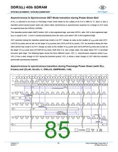
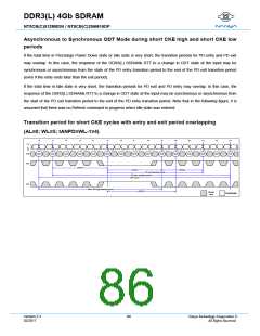
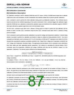
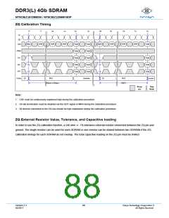
DDR3(L) 4Gb SDRAM
NT5CB(C)512M8DN / NT5CB(C)256M16DP
Absolute Maximum Ratings
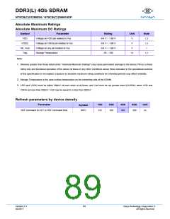
Absolute Maximum DC Ratings
Symbol
Parameter
Voltage on VDD pin relative to Vss
Voltage on VDDQ pin relative to Vss
Voltage on any pin relative to Vss
Storage Temperature
Rating
Unit
V
Note
1,3
1,3
1
VDD
-0.4 V ~ 1.80 V
-0.4 V ~ 1.80 V
-0.4 V ~ 1.80 V
-55 ~ 150
VDDQ
Vin, Vout
Tstg
V
V
1,2
C
Note:
1. Stresses greater than those listed under "Absolute Maximum Ratings" may cause permanent damage to the device.This is a stress
rating only and functional operation of the device at these or any other conditions above those indicated in the operational sections
of this specification is not implied. Exposure to absolute maximum rating conditions for extended periods may affect reliability.
2. Storage Temperature is the case surface temperature on the center/top side of the DRAM.
3. VDD and VDDQ must be within 300mV of each other at all times; and Vref must be not greater than 0.6VDDQ, when VDD and
VDDQ are less than 500mV; Vref may be equal to or less than 300mV.
Refresh parameters by device density
Parameter
1Gb
2Gb
4Gb
8Gb
Unit
Symbol
REF command to ACT or REF command time
tRFC
110
160
260
350
ns
Version 2.3
02/2017
89
Nanya Technology Cooperation ©
All Rights Reserved.

 NANYA [ Nanya Technology Corporation. ]