DDR3(L) 4Gb SDRAM
NT5CB(C)512M8DN / NT5CB(C)256M16DP
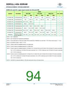
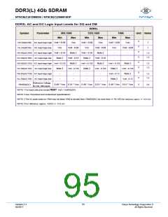
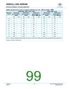
DDR3L AC and DC Logic Input Levels for DQ and DM
DDR3L
Symbol
Parameter
800,1066
1333,1600
1866
Unit Notes
Min
Max
Min
Max
Min
Max
V
V
VIH.DQ(DC90) DC input logic high Vref + 0.09
VIL.DQ(DC90) DC input logic low VSS
VIH.DQ(AC160) AC input logic high Vref + 0.16
VIL.DQ(AC160) AC input logic low Note 2
VIH.DQ(AC135) AC input logic high Vref + 0.135
VDD
Vref + 0.09
VSS
VDD
Vref + 0.09
VSS
VDD
1
1
Vref - 0.09
Note 2
Vref - 0.16
Note 2
Vref - 0.135
-
Vref - 0.09
Note 2
Vref - 0.16
Note 2
Vref - 0.135
-
Vref - 0.09
-
V
Vref + 0.16
Note 2
Vref + 0.135
Note 2
-
-
1,2
V
V
V
V
V
1,2
-
-
Vref + 0.135
Note 2
Vref + 0.13
Note 2
Note 2
Vref - 0.135
Note 2
Vref - 0.13
1,2
1,2
VIL.DQ(AC135) AC input logic low
VIH.DQ(AC130) AC input logic high
VIL.DQ(AC130) AC input logic low
Note 2
-
-
1,2
1,2
-
-
-
Reference Voltage
VRefDQ(DC)
0.49 * VDD 0.51 * VDD 0.49 * VDD 0.51 * VDD 0.49 * VDD 0.51 * VDD
V
3,4
for DQ, DM inputs
NOTE 1 For input only pins except REET. Vref = VrefDQ(DC).
NOTE 2 See “Overshoot and Undershoot Specifications”.
NOTE 3 The AC peak noise on VRef may not allow VRef to deviate from VRefDQ(DC) by more than +/-1% VDD (for reference: approx. +/- 13.5 mV).
NOTE 4 For reference: approx. VDD/2 +/- 13.5 mV.
Version 2.3
02/2017
95
Nanya Technology Cooperation ©
All Rights Reserved.

 NANYA [ Nanya Technology Corporation. ]