DDR3(L) 4Gb SDRAM
NT5CB(C)512M8DN / NT5CB(C)256M16DP
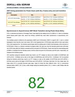
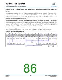
Asynchronous to Synchronous ODT Mode transition during Power-Down Exit
If DLL is selected to be frozen in Precharge Power Down Mode by the setting of bit A12 in MR0 to “0”, there is also a
transition period around power down exit, where either synchronous or asynchronous response to a change in ODT must
be expected from the DDR3(L) SDRAM.
This transition period starts tANPD before CKE is first registered high, and ends tXPDLL after CKE is first registered high.
tANPD is equal to (WL -1) and is counted (backwards) from the clock cycle where CKE is first registered high.
ODT assertion during the transition period may result in an RTT change as early as the smaller of tAONPDmin and (ODT-
Lon*tCK+tAONmin) and as late as the larger of tAONPDmax and (ODTLon*tCK+tAONmax). ODT de-assertion during the tran-
sition period may result in an RTT change as early as the smaller of tAOFPDmin and (ODTLoff*tCK+tAOFmin) and as late as
the larger of tAOFPDmax and (ODToff*tCK+tAOFmax). Note that if AL has a large value, the range where RTT is uncertain
becomes quite large. The following figure shows the three different cases: ODT_C, asynchronous response before tANPD
;
ODT_B has a state change of ODT during the transition period; ODT_A shows a state change of ODT after the transition
period with synchronous response.
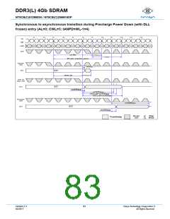
Asynchronous to synchronous transition during Precharge Power Down (with DLL
frozen) exit (CL=6; AL=CL-1; CWL=5; tANPD=WL-1=9)
T0
T1
T2
Ta0
Ta1
Ta2
Ta3
Ta4
Ta5
Ta6
Tb0
Tb1
Tb2
Tc0
Tc1
Tc2
Td0
Td1
CK
CK
CKE
CMD
NOP
NOP
NOP
NOP
NOP
NOP
NOP
NOP
NOP
NOP
NOP
NOP
NOP
NOP
tANPD
tXPDLL
PD exit transition period
ODT_C
_sync
tAOFPDmin
tAOFPDmax
DRAM
_RTT_
C_sync
RTT
ODT_B
_tran
tAOFPDmin
DRAM
_RTT_
B_tran
RTT
tAOFPDmax
ODTLoff + tAOFmin
ODTLoff + tAOFmax
ODTLoff
ODT_A
_async
tAOFmax
tAOFmin
DRAM_
RTT_A_
async
RTT
Do not
care
Time
Break
Transitioning
Version 2.3
02/2017
85
Nanya Technology Cooperation ©
All Rights Reserved.

 NANYA [ Nanya Technology Corporation. ]