DDR3(L) 4Gb SDRAM
NT5CB(C)512M8DN / NT5CB(C)256M16DP
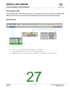
Mode Register MR3
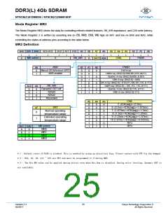
The Mode Register MR3 controls Multi-purpose registers. The Mode Register 3 is written by asserting low on , RA, A,
WE high on BA1 and BA0, and low on BA2 while controlling the states of address pins according to the table below.
MR3 Definition
BA2 BA1 BA0
A15-A13
A12 A11 A10 A9
A8
A7
A6
A5
A4
A3
A2
↓
A1
A0
↓
↓
↓
↓
↓
↓
↓
↓
↓
↓
↓
↓
↓
↓
↓
↓
MR select
0
MPR Loc
0
MPR
MPR
MPR Loc
Predefined pattern
Reserved
A2
0
1
A1
0
0
A0
0
1
Normal operation
Dataflow from MPR
Reserved
1
0
Reserved
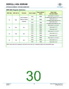
BA1 BA0 MR select
1
1
0
0
1
1
0
1
0
1
MR0
MR1
MR2
MR3
* 1 : BA2, A3 - A15 are RFU and must be programmed to 0 during MRS.
* 2 : The predefined pattern will be used for read synchronization.
* 3 : When MPR control is set for normal operation (MR3 A[2] = 0) then MR3 A[1:0] will be ignored.
Version 2.3
02/2017
27
Nanya Technology Cooperation ©
All Rights Reserved.

 NANYA [ Nanya Technology Corporation. ]