DDR3(L) 4Gb SDRAM
NT5CB(C)512M8DN / NT5CB(C)256M16DP
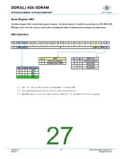
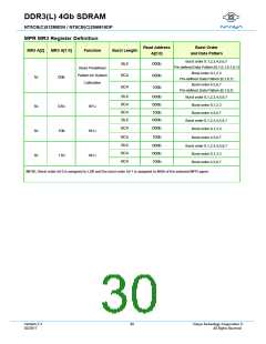
MPR MR3 Register Definition
Read Address
A[2:0]
Burst Order
MR3 A[2]
MR3 A[1:0]
Function
Burst Length
and Data Pattern
Burst order 0,1,2,3,4,5,6,7
Pre-defined Data Pattern [0,1,0,1,0,1,0,1]
Burst order 0,1,2,3
BL8
BC4
BC4
000b
000b
100b
Read Predefined
Pattern for System
Calibration
1b
00b
Pre-defined Data Pattern [0,1,0,1]
Burst order 4,5,6,7
Pre-defined Data Pattern [0,1,0,1]
BL8
BC4
BC4
BL8
000b
000b
100b
000b
Burst order 0,1,2,3,4,5,6,7
Burst order 0,1,2,3
1b
1b
1b
01b
10b
11b
RFU
RFU
RFU
Burst order 4,5,6,7
Burst order 0,1,2,3,4,5,6,7
BC4
000b
Burst order 0,1,2,3
BC4
BL8
BC4
BC4
100b
000b
000b
100b
Burst order 4,5,6,7
Burst order 0,1,2,3,4,5,6,7
Burst order 0,1,2,3
Burst order 4,5,6,7
NOTE: Burst order bit 0 is assigned to LSB and the burst order bit 7 is assigned to MSB of the selected MPR agent.
Version 2.3
02/2017
30
Nanya Technology Cooperation ©
All Rights Reserved.

 NANYA [ Nanya Technology Corporation. ]