DDR3(L) 4Gb SDRAM
NT5CB(C)512M8DN / NT5CB(C)256M16DP
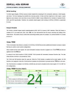
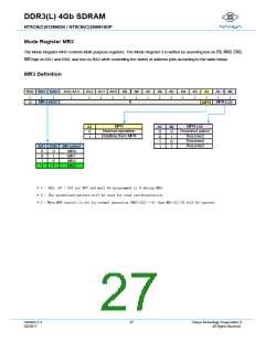
Multi-Purpose Register (MPR)
The Multi Purpose Register (MPR) function is used to Read out a predefined system timing calibration bit sequence.
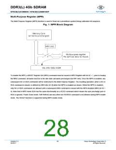
Fig. 1: MPR Block Diagram
To enable the MPR, a MODE Register Set (MRS) command must be issued to MR3 Register with bit A2 = 1, prior to issuing
the MRS command, all banks must be in the idle state (all banks precharged and tRP met). Once the MPR is enabled, any
subsequent RD or RDA commands will be redirected to the Multi Purpose Register. The resulting operation, when a RD or
RDA command is issued, is defined by MR3 bits A[1:0] when the MPR is enabled as shown. When the MPR is enabled,
only RD or RDA commands are allowed until a subsequent MRS command is issued with the MPR disabled (MR3 bit A2 =
0). Note that in MPR mode RDA has the same functionality as a READ command which means the auto precharge part of
RDA is ignored. Power-Down mode, Self-Refresh and any other non-RD/RDA command is not allowed during MPR enable
mode. The RESET function is supported during MPR enable mode.
Version 2.3
02/2017
28
Nanya Technology Cooperation ©
All Rights Reserved.

 NANYA [ Nanya Technology Corporation. ]