NTC Proprietary
Level: Property
DDR3(L)-2Gb SDRAM
NT5CB(C)256M8JQ/NT5CB(C)128M16JR
DDR3(L)-1600
Min. Max.
DDR3(L)-1866
DDR3-2133
Unit
Parameter
Symbol
Min.
Max.
Min.
Max.
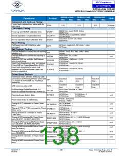
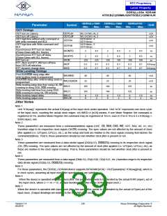
ODT Timings
ODT turn on Latency
ODT turn off Latency
ODTLon
ODTLoff
WL-2=CWL+AL-2
WL-2=CWL+AL-2
ODTH4min.: 4
ODTH4max.: -
ODTH8min.: 6
ODTH8max.: -
nCK
nCK
ODT high time without write command or
with write command and BC4
ODT high time with Write command and
BL8
Asynchronous RTT turn-on delay
(Power-Down with DLL frozen)
Asynchronous RTT turn-off delay
(Power-Down with DLL frozen)
RTT turn-on
ODTH4
nCK
nCK
ns
ODTH8
tAONPD
2
8.5
2
8.5
2
8.5
tAOFPD
tAON
2
8.5
225
0.7
0.7
2
8.5
195
0.7
0.7
2
8.5
180
0.7
0.7
ns
-225
0.3
0.3
-195
0.3
0.3
-180
0.3
0.3
ps
RTT_Nom and RTT_WR turn-off time
from ODTLoff reference
RTT dynamic change skew
tAOF
tCK(avg)
tCK(avg)
tADC
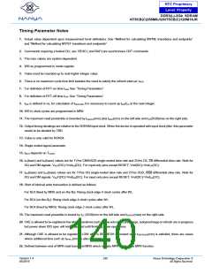
Write Leveling Timings
First DQS/ rising edge after
write leveling mode is programmed
DQS/ delay after write leveling mode is
programmed
Write leveling setup time from rising CK,
crossing to rising DQS, crossing
Write leveling hold time from rising DQS,
crossing to rising CK, crossing
Write leveling output delay
tWLMRD
tWLDQSEN
tWLS
40
25
-
-
-
-
40
25
-
-
-
-
40
25
-
-
-
-
nCK
nCK
ps
165
165
140
140
125
125
tWLH
ps
tWLO
tWLOE
0
0
7.5
2
0
0
7.5
2
0
0
7.5
2
ns
ns
Write leveling output error
Jitter Notes
Note 1
Unit “tCK(avg)” represents the actual tCK(avg) of the input clock under operation. Unit “nCK” represents one clock cycle
of the input clock, counting the actual clock edges. ex) tMRD=4 [nCK] means; if one Mode Register Set command is
registered at Tm, another Mode Register Set command may be registered at Tm+4, even if (Tm+4-Tm) is 4 x tCK(avg) +
tERR (4per), min.
Note 2
These parameters are measured from a command/address signal (CKE, , RA, A, WE, ODT, BA0, A0, A1, etc)
transition edge to its respective clock signal (CK/) crossing. The spec values are not affected by the amount of clock
jitter applied (i.e. tJIT(per), tJIT(cc), etc.), as the setup and hold are relative to the clock signal crossing that latches the
command/address. That is, these parameters should be met whether clock jitter is present or not.
Note 3
These parameters are measured from a data strobe signal (DQS(L/U), LU)) crossing to its respective clock signal
(CK, ) crossing. The spec values are not affected by the amount of clock jitter applied (i.e. tJIT(per), tJIT(cc), etc), as
these are relative to the clock signal crossing. That is, these parameters should be met whether clock jitter is present or
not.
Note 4
These parameters are measured from a data signal (DM(L/U), DQ(L/U)0, DQ(L/U)1, etc.) transition edge to its respective
data strobe signal (DQS(L/U), LU) crossing.
Note 5
For these parameters, the DDR3(L) SDRAM device supports tnPARAM [nCK] = RU{Tparam[ns] / tCK(avg)[ns]}, which is
in clock cycles, assuming all input clock jitter specifications are satisfied.
Note 6
When the device is operated with input clock jitter, this parameter needs to be derated by the actual tERR (mper), act of
the input clock, where 2 <= m <=12. (Output derating is relative to the SDRAM input clock.)
Note 7
When the device is operated with input clock jitter, this parameter needs to be derated by the actual tJIT(per),act of the
input clock. (Output deratings are relative to the SDRAM input clock.)
Version 1.4
05/2019
139
Nanya Technology Cooperation ©
All Rights Reserved.

 NANYA [ Nanya Technology Corporation. ]