NTC Proprietary
Level: Property
DDR3(L)-2Gb SDRAM
NT5CB(C)256M8JQ/NT5CB(C)128M16JR
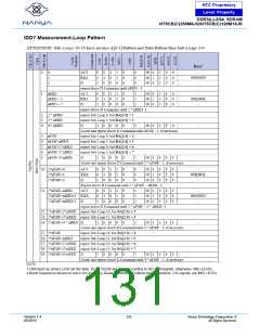
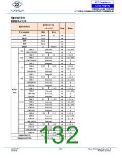
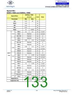
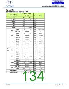
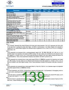
Speed Bin Notes
NOTE 1. The CL setting and CWL setting result in tCK(AVG).MIN and tCK(AVG).MAX requirements. When making a selection of
tCK(AVG), both need to be fulfilled: Requirements from CL setting as well as requirements from CWL setting.
NOTE 2. tCK(AVG).MIN limits: Since CAS Latency is not purely analog - data and strobe output are synchronized by the DLL - all
possible intermediate frequencies may not be guaranteed. An application should use the next smaller JEDEC standard
tCK(AVG) value (3.0, 2.5, 1.875, 1.5, 1.25, 1.07, or 0.938 ns) when calculating CL [nCK] = tAA [ns] / tCK(AVG) [ns], rounding
up to the next ‘Supported CL’, where tCK(AVG) = 3.0 ns should only be used for CL = 5 calculation.
NOTE 3. tCK(AVG).MAX limits: Calculate tCK(AVG) = tAA.MAX / CL SELECTED and round the resulting tCK(AVG) down to the next
valid speed bin (i.e. 3.3ns or 2.5ns or 1.875 ns or 1.5 ns or 1.25 ns or 1.07 ns or 0.938 ns). This result is tCK(AVG).MAX
corresponding to CL SELECTED.
NOTE 4. ‘Reserved’ settings are not allowed. User must program a different value.
NOTE 5. ‘Optional’ settings allow certain devices in the industry to support this setting, however, it is not a mandatory feature. Refer to
supplier’s data sheet and/or the DIMM SPD information if and how this setting is supported.
NOTE 6. Any DDR3-1066 speed bin also supports functional operation at lower frequencies as shown in the table which are not
subject to Production Tests but has verified.
NOTE 7. Any DDR3-1333 speed bin also supports functional operation at lower frequencies as shown in the table which are not
subject to Production Tests but has verified.
NOTE 8. Any DDR3-1600 speed bin also supports functional operation at lower frequencies as shown in the table which are not
subject to Production Tests but has verified.
NOTE 9. Any DDR3-1866 speed bin also supports functional operation at lower frequencies as shown in the table which are not
subject to Production Tests but has verified.
NOTE 10. Any DDR3-2133 speed bin also supports functional operation at lower frequencies as shown in the table which are not
subject to Production Tests but has verified.
NOTE 11. For devices supporting optional down binning to CL=7 and CL=9, tAA/tRCD/tRPmin must be 13.125 ns. SPD settings must
be programmed to match. For example, DDR3-1333(9-9-9) devices supporting down binning to DDR3-1066(7-7-7) should
program 13.125 ns in SPD bytes for tAAmin (Byte 16), tRCDmin (Byte 18), and tRPmin (Byte 20). DDR3-1600(11-11-11)
devices supporting down binning to DDR3-1333(9-9-9) or DDR3-1066(7-7-7) should program 13.125 ns in SPD bytes for
tAAmin (Byte16), tRCDmin (Byte 18), and tRPmin (Byte 20). Once tRP (Byte 20) is programmed to 13.125ns, tRCmin (Byte
21,23) also should be programmed accodingly. For example, 49.125ns (tRASmin + tRPmin = 36 ns + 13.125 ns) for DDR3-
1333(9-9-9) and 48.125ns (tRASmin + tRPmin = 35 ns + 13.125 ns) for DDR3-1600(11-11-11).
NOTE 12. DDR3 800 AC timing apply if DRAM operates at lower than 800 MT/s data rate.
NOTE 13. For CL5 support, refer to DIMM SPD information. DRAM is required to support CL5. CL5 is not mandatory in SPD coding.
NOTE 14. For devices supporting optional down binning to CL=11, CL=9 and CL=7, tAA/tRCD/tRPmin must be 13.125ns. SPD setting
must be programed to match. For example, DDR3-1866(13-13-13) devices supporting down binning to DDR3-1600(11-11-
11) or DDR3-1333(9-9-9) or 1066(7-7-7) should program 13.125ns in SPD bytes for tAAmin(byte16), tRCDmin(Byte18) and
tRPmin (byte20). Once tRP (Byte 20) is programmed to 13.125ns, tRCmin (Byte 21,23) also should be programmed
accordingly. For example, 47.125ns (tRASmin + tRPmin = 34 ns+ 13.125 ns).
NOTE 15. Supporting CL setting herewith is a reference base on JEDEC's. Precise CL & tCK setting needs to follow where defined on
speed compatible table in section “Operating frequency”, exceptional setting please confirm with NTC.CWL setting follow CL
value in above table in section “Speed Bin”
Version 1.4
05/2019
135
Nanya Technology Cooperation ©
All Rights Reserved.

 NANYA [ Nanya Technology Corporation. ]