NTC Proprietary
Level: Property
DDR3(L)-2Gb SDRAM
NT5CB(C)256M8JQ/NT5CB(C)128M16JR
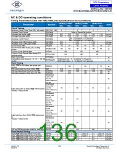
AC & DC operating conditions
Timing Parameters (Data rate 1600,1866,2133 specifications and conditions)
DDR3(L)-1600
DDR3(L)-1866
DDR3-2133
Parameter
Symbol
Unit
Min.
Max.
Min.
Max.
Min.
Max.
Clock Timing
Minimum Clock Cycle Time (DLL off mode) tCK (DLL_off)
8
-
8
-
8
-
ns
Average Clock Period
Average high pulse width
Average low pulse width
tCK(avg)
tCH(avg)
tCL(avg)
Refer to “Speed Bin”section
0.47
0.47
0.53
0.53
0.47
0.47
0.53
0.53
0.47
0.47
0.53
0.53
tCK(avg)
tCK(avg)
Min.: tCK(avg)min + tJIT(per)min
Max.: tCK(avg)max + tJIT(per)max
Absolute Clock Period
tCK(abs)
Absolute clock HIGH pulse width
Absolute clock LOW pulse width
Clock Period Jitter
tCH(abs)
tCL(abs)
JIT(per)
0.43
0.43
-70
-
-
70
0.43
0.43
-60
-
-
60
0.43
0.43
-50
-
-
50
tCK(avg)
tCK(avg)
ps
Clock Period Jitter during DLL locking
period
Cycle to Cycle Period Jitter
Cycle to Cycle Period Jitter during DLL
locking period
Duty Cycle Jitter
Cumulative error across n = 2, 14 . . . 49, 50
cycles
JIT(per, lck)
tJIT(cc)
-60
60
-50
50
-40
40
ps
140
120
120
100
100
80
JIT(cc, lck)
tJIT(duty)
tERR(nper)
-
-
-
-
-
-
ps
ps
tERR(nper) min = (1 + 0.68ln(n)) * tJIT(per)min
tERR (nper) max = (1 + 0.68ln(n)) * tJIT (per)max
Data Timing
DQS, to DQ skew, per group, per
access
tDQSQ
-
100
-
85
-
75
ps
DQ output hold time from DQS,
DQ low-impedance time from CK,
DQ high impedance time from CK,
tQH
0.38
-450
-
-
0.38
-390
-
-
0.38
-360
-
-
tCK(avg)
tLZ(DQ)
tHZ(DQ)
tDS(base)
DDR3-1600
(AC175)
225
225
195
195
180
180
ps
ps
-
-
-
-
-
-
-
-
-
ps
ps
DDR3-1866/2133
(AC150)
tDS(base)
DDR3-1600
(AC150)
10
68
53
Data setup time to DQS, referenced to
Vih(ac) / Vil(ac) levels
DDR3-1866/2133
(AC135)
tDS(base)
DDR3L-1600
(AC135)
SR=1V/ns
25
45
-
-
70
70
-
-
-
-
-
ps
ps
DDR3L-1866
(AC130)
SR=2V/ns
tDH(base)
DC100
DDR3-1600
SR=1V/ns
55
DDR3-1866/2133
SR=2V/ns
Data hold time from DQS, referenced
to
Vih(dc) / Vil(dc) levels
tDH(base)
DC90
DDR3L-1600
SR=1V/ns
DDR3L-1866
SR=2V/ns
55
-
-
75
-
-
-
-
-
ps
ps
DQ and DM Input pulse width for each input tDIPW
360
320
280
Data Strobe Timing
DQS, differential READ Preamble
DQS, differential READ Postamble
DQS, differential output high time
DQS, differential output low time
tRPRE
tRPST
tQSH
tQSL
0.9
0.3
0.4
0.4
Note 19
Note 11
0.9
0.3
0.4
0.4
Note 19
Note 11
0.9
0.3
0.4
0.4
Note 19 tCK(avg)
Note 11 tCK(avg)
-
-
-
-
-
-
tCK(avg)
tCK(avg)
Version 1.4
05/2019
136
Nanya Technology Cooperation ©
All Rights Reserved.

 NANYA [ Nanya Technology Corporation. ]