NTC Proprietary
Level: Property
DDR3(L)-2Gb SDRAM
NT5CB(C)256M8JQ/NT5CB(C)128M16JR
DDR3(L)-1600
DDR3(L)-1866
DDR3-2133
Unit
Parameter
Symbol
Min.
Max.
Min.
Max.
Min.
Max.
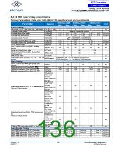
Data Strobe Timing
DQS, differential WRITE Preamble
DQS, differential WRITE Postamble
DQS, rising edge output access time
from rising CK,
DQS and low-impedance time
(Referenced from RL – 1)
tWPRE
tWPST
0.9
0.3
-
-
0.9
0.3
-
-
0.9
0.3
-
-
tCK(avg)
tCK(avg)
tDQSCK
-225
-450
-
225
225
225
-195
-390
-
195
195
195
-180
-360
-
180
180
180
ps
ps
ps
tLZ(DQS)
tHZ(DQS)
DQS and high-impedance time
(Referenced from RL + BL/2)
DQS, differential input low pulse width tDQSL
DQS, differential input high pulse width tDQSH
0.45
0.45
0.55
0.55
0.45
0.45
0.55
0.55
0.45
0.45
0.55
0.55
tCK(avg)
tCK(avg)
DQS, rising edge to CK, rising
edge
DQS, falling edge setup time to
CK, rising edge
DQS, falling edge hold time from
CK, rising edge
tDQSS
-0.27
0.18
0.18
0.27
-0.27
0.18
0.18
0.27
-0.27
0.18
0.18
0.27
tCK(avg)
tCK(avg)
tCK(avg)
tDSS
-
-
-
-
-
-
tDSH
Command and Address Timing
DLL locking time
tDLLK
tRTP
512
-
512
-
512
-
nCK
Internal READ Command to
PRECHARGE Command delay
Delay from start of internal write
transaction to internal read command
WRITE recovery time
tRTPmin.: max(4tCK, 7.5ns)
tRTPmax.: -
tWTRmin.: max(4tCK, 7.5ns)
tWTRmax.: -
tWTR
tWR
tMRD
15
4
-
-
15
4
-
-
15
4
-
-
ns
Mode Register Set command cycle time
nCK
tMODmin.: max(12tCK, 15ns)
tMODmax.:
Mode Register Set command update delay tMOD
ACT to internal read or write delay time
PRE command period
tRCD
tRP
tRC
Refer to “Speed Bin” section
ACT to ACT or REF command period
ACTIVE to PRECHARGE command period tRAS
A to A command delay
Auto precharge write recovery + precharge
time
tCCD
4
-
4
-
4
-
nCK
nCK
nCK
tDAL(MIN)
tMPRR
WR + roundup(tRP / tCK(avg))
Multi-Purpose Register Recovery Time
1
-
1
-
1
-
max(4tCK
,6ns)
max(4tCK
,5ns)
max(4tCK
,5ns)
ACTIVE to ACTIVE command period
(1KB page size)
tRRD
tRRD
-
-
-
max(4tCK
max(4tCK
max(4tCK
ACTIVE to ACTIVE command period
(2KB page size)
-
-
-
,7.5ns)
30
,6ns)
27
,6ns)
25
Four activate window (1KB page size)
Four activate window (2KB page size)
tFAW
tFAW
-
-
-
-
-
-
ns
ns
40
35
35
tIS(BASE)
DDR3-1600
(AC175)
45
-
-
-
-
-
-
-
-
ps
ps
DDR3-1866/2133
(AC150)
tIS(BASE)
DDR3-1600
(AC150)
170
150
135
Command and Address setup time to CK,
referenced to Vih(ac) / Vil(ac) levels
DDR3-1866/2133
(AC125)
tIS(BASE)
DDR3L (AC160)
tIS(BASE)
DDR3L (AC135)
tIS(BASE)
DDR3L (AC125)
60
185
-
-
-
-
-
-
-
-
-
-
-
-
-
ps
ps
ps
65
150
tIH(BASE)
DDR3 (DC100)
120
130
-
-
100
110
-
-
95
-
-
-
ps
ps
Command and Address hold time from CK,
referenced to Vih(dc) / Vil(dc) levels
tIH(BASE)
DDR3L(DC90)
Version 1.4
05/2019
137
Nanya Technology Cooperation ©
All Rights Reserved.

 NANYA [ Nanya Technology Corporation. ]