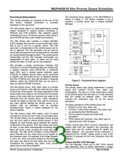
MUPA64K16 Alto Priority Queue Scheduler
Table 1: Pin Description
Signal
Name
REG[2.0]
Function
Input
Function
Register Select. Selects the register to be read or written during a DQ[31:0] bus
operation.
Instruction Bus OP[2:0] selects the operation to be performed. See Table 5 showing op
codes for a list of legal values.
OP[2:0]
PQ[3.0]
/W
Input
Priority Queue Select. Selects the priority queue to which an operation applied. Note
that some operations, such as Noop, do not use this value.
Input
Input
Input
Read/Write. /W enables a register write or an operation that inputs data, such as Insert,
depending on the value of OP[2:0].
Chip Select. /CS indicates to the device that a new command is available on OP[2:0],
REG[2:0], PQ[3:0] and /W. If /W is zero, then /CS also indicates that there is new data
on the DQ[31:0]. /CS must be synchronous to CLK.
/CS
Status Register. Provides device status information; equivalent to bits 4:0 of the Status
Register (see Table 2).
Device clock. All internal operations and interface timings are synchronized to the rising
edge of the clock.
STR[4:0]
CLK
Output
Input
System Reset. The PLL in Alto requires 100 microseconds to stabilize after reset and
no commands should be issued during this time. Also, the UID manager requires an
additional 2200 clock cycles to initialize after this 100 microsecond interval.
Associated Data Bus. This bus outputs the associated data for interface to external
RAM. The contents of both the IDR and MDR are made available on this bus, selected
by ADS.
/RST
Input
AD[15:0]
/ADV
Output
Output
Associated Data Bus Valid. ADV indicates the validity of the AD[15:0] bus. AD[15:0] is
invalid when ADS=1 and a peek or extract operation is performed on an empty priority
queue. /ADV signal is an address bit AD[16] of the Associated Data Bus, however,
AD[16] is not a part of the SRAM address.
Associated Data Bus Select. ADS determines whether the AD[15:0] bus carries the
value of the IDR (ADS=0) or the MDR (ADS=1).
Associated Data Bus Output Enable. /ADOE asynchronously enables Alto to drive the
AD[15:0] bus.
ADS
Input
Input
/ADOE
Data Bus. The bi-directional data bus writes to and reads from the registers. Data for
registers that are less than 32 bits occupy the least significant bits of DQ[31:0].
Data Bus Output Enable. Asynchronously enables the device to drive the DQ[31:0]
DQ[31:0]
/DQOE
Input/Output
Input
pins.
READY. RDY indicates that the bus is idle and able to accept a new command.
JTAG reset pin.
JTAG Test Clock.
JTAG Test Mode Select.
JTAG Test data Input.
JTAG Test Data Output.
Supply Voltage for Core (1.8V)
Supply Voltage for I/O (3.3V)
Ground
/RDY
/TRST
TCLK
TMS
TDI
TDO
VDD
VDDQ
VSS
Input
Input
Input
Input
Input
Output
Power
Power
GND
Input
GND
AVDD
AVSS
Supply Voltage for PLL (1.8V)
Ground for PLL
MUSIC Semiconductors Confidential
2
Rev 0.3 Draft

 MUSIC [ MUSIC SEMICONDUCTORS ]