NB671, 24V, HIGH CURRENT SYNCHRONOUS STEP-DOWN CONVERTER
Therefore, when EN is driven by an external logic
Over Current Protection
signal, the EN voltage should be lower than 12V;
when EN is connected with VIN through a pull-up
resistor or a resistive voltage divider, the
resistance selection should ensure the maximum
pull up current less than 1mA.
NB671 has cycle-by-cycle over current limiting
control. The current-limit circuit employs a
"valley" current-sensing algorithm. The part uses
the Rds(on) of the low side MOSFET as a
current-sensing element. If the magnitude of the
current-sense signal is above the current-limit
threshold, the PWM is not allowed to initiate a
new cycle.
If using a resistive voltage divider and VIN higher
than 12V, the allowed minimum pull-up resistor
Rup should meet the following equation:
V -12V 12V
IN
The trip level is fixed internally. The inductor
current is monitored by the voltage between GND
pin and SW pin. GND is used as the positive
current sensing node so that GND should be
connected to the source terminal of the bottom
MOSFET.
(10)
-
=1mA
Rup
Rdown
Especially, just using the pull-up resistor Rup(the
pull-down resistor is not connected), the
IN-START is determined by input UVLO, and the
V
minimum resistor value is:
Since the comparison is done during the high
side MOSFET OFF and low side MOSFET ON
state, the OC trip level sets the valley level of the
inductor current. Thus, the load current at over-
current threshold, IOC, can be calculated as
follows:
V -12V
IN
(11)
Rup =
(W)
1mA
A typical pull-up resistor is 499kΩ.
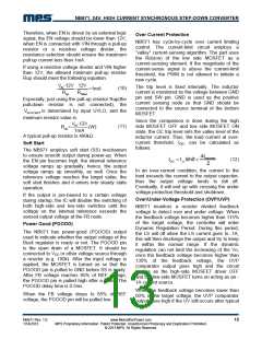
Soft Start
The NB671 employs soft start (SS) mechanism
to ensure smooth output during power-up. When
the EN pin becomes high, the internal reference
voltage ramps up gradually; hence, the output
voltage ramps up smoothly, as well. Once the
reference voltage reaches the target value, the
soft start finishes and it enters into steady state
operation.
ΔI
inductor
IOC = I_limit +
(12)
2
In an over-current condition, the current to the
load exceeds the current to the output capacitor;
thus the output voltage tends to fall off.
Eventually, it will end up with crossing the under
voltage protection threshold and shutdown.
If the output is pre-biased to a certain voltage
during startup, the IC will disable the switching of
both high-side and low-side switches until the
voltage on the internal reference exceeds the
sensed output voltage at the FB node.
Over/Under-Voltage Protection (OVP/UVP)
NB671 monitors a resistor divided feedback
voltage to detect over and under voltage. When
the feedback voltage becomes higher than 115%
of the target voltage, the controller will enter
Dynamic Regulation Period. During this period,
the LS will off when the LS current goes to -1A,
this will then discharge the output and try to keep
it within the normal range. If the dynamic
regulation can not limit the increasing of the Vo,
once the feedback voltage becomes higher than
130% of the feedback voltage, the OVP
comparator output goes high and the circuit
latches as the high-side MOSFET driver OFF
and the low-side MOSFET turns on acting as an -
1A current source.
Power Good (PGOOD)
The NB671 has power-good (PGOOD) output
used to indicate whether the output voltage of the
Buck regulator is ready or not. The PGOOD pin
is the open drain of a MOSFET. It should be
connected to VCC or other voltage source through
a resistor (e.g. 100k). After the input voltage is
applied, the MOSFET is turned on so that the
PGOOD pin is pulled to GND before SS is ready.
After FB voltage reaches 95% of REF voltage,
the PGOOD pin is pulled high after a delay. The
PGOOD delay time is 0.5ms.
When the feedback voltage becomes lower than
60% of the target voltage, the UVP comparator
output goes high if the UV still occurs after typical
When the FB voltage drops to 85% of REF
voltage, the PGOOD pin will be pulled low.
NB671 Rev. 1.0
1/14/2013
www.MonolithicPower.com
MPS Proprietary Information. Patent Protected. Unauthorized Photocopy and Duplication Prohibited.
© 2013 MPS. All Rights Reserved.
13

 MPS [ MONOLITHIC POWER SYSTEMS ]