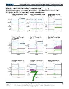
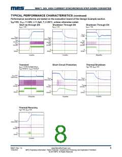
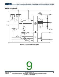
NB671, 24V, HIGH CURRENT SYNCHRONOUS STEP-DOWN CONVERTER
As the output current increases from the light
resistor. Ceramic capacitors usually can not be
used as output capacitor.
load condition, the time period within which the
current modulator regulates becomes shorter.
The HS-FET is turned ON more frequently.
Hence, the switching frequency increases
correspondingly. The output current reaches the
critical level when the current modulator time is
zero. The critical level of the output current is
determined as follows:
To realize the stability, the ESR value should be
chosen as follow:
TSW
TON
2
+
0.7× π
(2)
RESR
≥
COUT
TSW is the switching period.
(VIN − VOUT)× VOUT
2×L×FSW × VIN
(1)
IOUT
=
The NB671 has built in internal ramp
compensation to make sure the system is stable
even without the help of output capacitor’s ESR;
and thus the pure ceramic capacitor solution can
be applicant. The pure ceramic capacitor solution
can significantly reduce the output ripple, total
BOM cost and the board area.
It turns into PWM mode once the output current
exceeds the critical level. After that, the switching
frequency stays fairly constant over the output
current range.
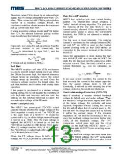
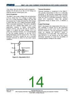
Jitter and FB Ramp Slope
Jitter occurs in both PWM and skip modes when
noise in the VFB ripple propagates a delay to the
HS-FET driver, as shown in Figures 4 and 5.
Jitter can affect system stability, with noise
immunity proportional to the steepness of VFB’s
downward slope. However, VFB ripple does not
directly affect noise immunity.
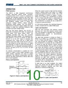
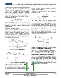
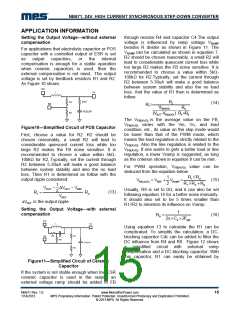
Figure 6 shows a typical output circuit in PWM
mode without an external ramp circuit. Turn to
application information section for design steps
without external compensation.
VSLOPE1
VNOISE
VFB
VREF
HSDriver
Figure 6—Simplified Circuit in PWM Mode
without External Ramp Compensation
Jitter
Figure 4—Jitter in PWM Mode
When using a large-ESR capacitor on the output,
add a ceramic capacitor with a value of 10uF or
less to in parallel to minimize the effect of ESL.
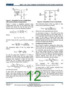
VSLOPE2
VNOISE
VFB
Operating with external ramp compensation
VREF
The NB671 is usually able to support ceramic
output capacitors without external ramp, however,
in some of the cases, the internal ramp may not
be enough to stabilize the system, and external
ramp compensation is needed. Skip to
application information section for design steps
with external ramp compensation.
HSDriver
Jitter
Figure 5—Jitter in Skip Mode
Operating without external ramp
The traditional constant-on-time control scheme
is intrinsically unstable if output capacitor’s ESR
is not large enough as an effective current-sense
NB671 Rev. 1.0
1/14/2013
www.MonolithicPower.com
MPS Proprietary Information. Patent Protected. Unauthorized Photocopy and Duplication Prohibited.
© 2013 MPS. All Rights Reserved.
11

 MPS [ MONOLITHIC POWER SYSTEMS ]