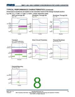
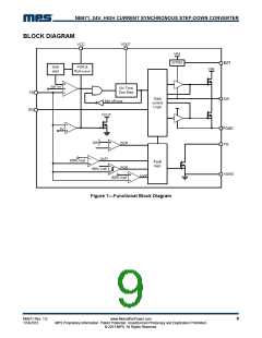
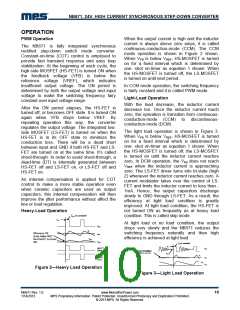
NB671, 24V, HIGH CURRENT SYNCHRONOUS STEP-DOWN CONVERTER
Vo
ESR
R1
FB
Ro
Cout
R2
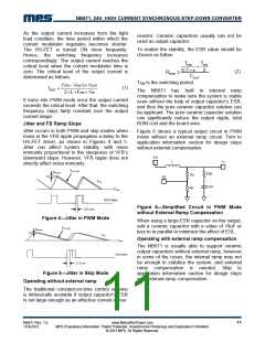
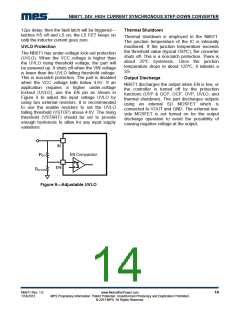
Figure 7—Simplified Circuit in PWM Mode
with External Ramp Compensation
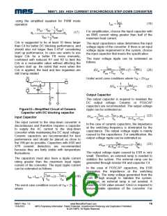
Figure 8—Simplified Circuit in skip Mode
The downward slope of the VFB ripple in skip
mode can be determined as follow:
Figure 7 shows a simplified external ramp
compensation (R4 and C4) for PWM mode, with
HS-FET off. Chose R1, R2, R9 and C4 of the
external ramp to meet the following condition:
−VREF
(8)
VSLOPE2
=
( R +R //Ro)×C
(
)
1
2
OUT
⎛
⎜
⎝
⎞
⎟
⎠
R1 ×R2
R1 + R2
1
1
5
Where Ro is the equivalent load resistor.
<
×
+ R9
(3)
2π×FSW × C4
As described in Figure 5, VSLOPE2 in the skip
mode is lower than that is in the PWM mode, so
it is reasonable that the jitter in the skip mode is
larger. If one wants a system with less jitter
during light load condition, the values of the VFB
resistors should not be too big, however, that will
decrease the light load efficiency.
Where:
IR4 = IC4 +IFB ≈ IC4
(4)
And the Vramp on the VFB can then be estimated
as:
Configuring the EN Control
V − VOUT
R4 ×C4
R1 //R2
IN
(5)
VRAMP
=
×TON ×
R1 //R2 +R9
EN is used to enable or disable the whole chip.
Pull En high to turn on the regulator and pull EN
low to turn it off. Do not float the pin.
The downward slope of the VFB ripple then
follows
For automatic start-up the EN pin can be pulled
up to input voltage through a resistive voltage
divider. Choose the values of the pull-up resistor
(Rup from Vin pin to EN pin) and the pull-down
resistor (Rdown from EN pin to GND) to
determine the automatic start-up voltage:
−VRAMP
−VOUT
R4 ×C4
(6)
VSLOPE1
=
=
T
off
As can be seen from equation 6, if there is
instability in PWM mode, we can reduce either
R4 or C4. If C4 can not be reduced further due to
limitation from equation 3, then we can only
reduce R4. For a stable PWM operation, the
(Rup + Rdown
)
V
= 1.35×
(V)
(9)
IN−START
Rdown
V
slope1 should be design follow equation 7.
For
example,
for
Rup=150kΩ
and
TSW
T
+
ON -RESRCOUT
Io×10-3
TSW -Ton
Rdown=51kΩ,the VIN−START is set at 5.32V.
0.7×π
2
(7)
-Vslope1
≥
VOUT +
2×L×COUT
To avoid noise, a 10nF ceramic capacitor from
EN to GND is recommended.
Io is the load current.
There is an internal Zener diode on the EN pin,
which clamps the EN pin voltage to prevent it
from running away. The maximum pull up current
assuming a worst case 12V internal Zener clamp
should be less than 1mA.
In skip mode, the downward slope of the VFB
ripple is the same whether the external ramp is
used or not. Figure 8 shows the simplified circuit
of the skip mode when both the HS-FET and LS-
FET are off.
NB671 Rev. 1.0
1/14/2013
www.MonolithicPower.com
MPS Proprietary Information. Patent Protected. Unauthorized Photocopy and Duplication Prohibited.
© 2013 MPS. All Rights Reserved.
12

 MPS [ MONOLITHIC POWER SYSTEMS ]