Freescale Semiconductor, Inc.
Electrical Specifications
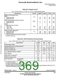
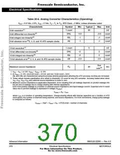
Table 20-6. Analog Converter Characteristics (Operating)
V
= 5.0 Vdc ±10%, V = 0 Vdc, T = T to T , ATD Clock = 2 MHz, unless otherwise noted
SS A L H
DD
Characteristic
Symbol
1 count
DNL
Min
Typical
Max
Unit
mV
(1)
20
8-bit resolution
(2)
−0.5
−1
+0.5
+1
count
count
count
8-bit differential non-linearity
(2)
INL
8-bit integral non-linearity
,(3)
AE
−1
+1
8-bit absolute error 2, 4, 8, and 16 ATD sample clocks
(1)
1 count
DNL
INL
5
mV
10-bit resolution
(2)
–2
–2
2
2
count
count
count
10-bit differential non-linearity
(2)
10-bit integral non-linearity
(3)
AE
–2.5
2.5
10-bit absolute error 2, 4, 8, and 16 ATD sample clocks
See
R
Maximum source impedance
20
KΩ
S
(4)
note
1. VRH − VRL ≥ 5.12V; VDDA − VSSA = 5.12V
2. At VREF = 5.12V, one 8-bit count = 20 mV, and one 10-bit count = 5mV.
INL and DNL are characterized using the process window parameters affecting the ATD accuracy, but they are not tested.
3. These values include quantization error which is inherently 1/2 count for any A/D converter. Accuracy tested when when
VRL=VSS, VRH=VDD and external source impedence is close to zero.
4. Maximum source impedance is application-dependent. Error resulting from pin leakage depends on junction leakage into
the pin and on leakage due to charge-sharing with internal capacitance.
Error from junction leakage is a function of external source impedance and input leakage current. Expected error in result
value due to junction leakage is expressed in voltage (VERRJ):
VERRJ = RS × IOFF
where IOFF is a function of operating temperature. Charge-sharing effects with internal capacitors are a function of ATD
clock speed, the number of channels being scanned, and source impedance. For 8-bit conversions, charge pump leakage
is computed as follows:
VERRJ = .25pF × VDDA × RS × ATDCLK/(8 × number of channels)
Advance Information
370
68HC(9)12D60 — Rev 4.0
MOTOROLA
Electrical Specifications
For More Information On This Product,
Go to: www.freescale.com

 MOTOROLA [ MOTOROLA ]