Freescale Semiconductor, Inc.
Electrical Specifications
Tables of Data
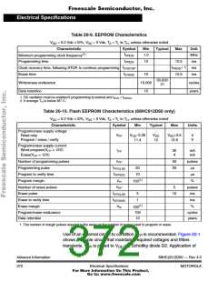
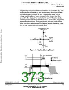
programming voltage via diode reverse-biases D2, protecting V from
DD
excessive reverse current. D2 also protects the FLASH from damage
should programming voltage go to 0. Programming power supply
voltage must be adjusted to compensate for the forward-bias drop
across D1. The charge time constant of R1 and C1 filters transients,
while R2 provides a discharge bleed path to C1. Allow for RC charge and
discharge time constants when applying and removing power. When
using this circuit, keep leakage from external devices connected to the
V
pin low, to minimize diode voltage drop.
FP
PROGRAMMING VOLTAGE
POWER SUPPLY
D1
R1
10Ω
D2
4.5V
VFP
PIN
VDD
R2
22kΩ
C1
0.1µF
Figure 20-1V Conditioning Circuit
FP
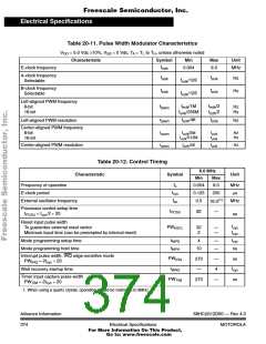
30ns MAXIMUM
13.5V
12.8V
VFP ENVELOPE
VDD ENVELOPE
11.4V
COMBINED VDD AND VFP
t
ER
6.5V
4.5V
4.15V
0V
–0.30V
PROGRAM
ERASE
VERIFY
NORMAL
READ
POWER
DOWN
POWER
ON
Figure 20-2V Operating Range
FP
68HC(9)12D60 — Rev 4.0
MOTOROLA
Advance Information
373
Electrical Specifications
For More Information On This Product,
Go to: www.freescale.com

 MOTOROLA [ MOTOROLA ]